CY8CTMG200-32LQXI Cypress Semiconductor Corp, CY8CTMG200-32LQXI Datasheet - Page 291
CY8CTMG200-32LQXI
Manufacturer Part Number
CY8CTMG200-32LQXI
Description
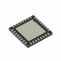
IC MCU 32K FLASH 32UQFN
Manufacturer
Cypress Semiconductor Corp
Series
TrueTouch™r
Datasheet
1.CY8CTST200-16LGXI.pdf
(308 pages)
Specifications of CY8CTMG200-32LQXI
Program Memory Type
FLASH (32 kB)
Package / Case
32-UQFN Exposed Pad, 32-HUQFN, 32-SQFN
Applications
Touchscreen Controller
Core Processor
M8C
Controller Series
CY8CT
Ram Size
2K x 8
Interface
I²C, SPI, UART/USART, USB
Number Of I /o
28
Voltage - Supply
1.8 V
Operating Temperature
-40°C ~ 85°C
Mounting Type
Surface Mount
Processor Series
CY8CTxx2xx
Core
M8C
Data Bus Width
8 bit
Data Ram Size
2 KB
Interface Type
I2C, SPI
Maximum Clock Frequency
24 MHz
Number Of Timers
3
Operating Supply Voltage
1.71 V to 5.5 V
Mounting Style
SMD/SMT
Program Memory Size
32 KB
Lead Free Status / RoHS Status
Lead free / RoHS Compliant
For Use With
770-1000 - ISP 4PORT FOR CYPRESS PSOC MCU
Lead Free Status / Rohs Status
Lead free / RoHS Compliant
Other names
428-2954
Available stocks
Company
Part Number
Manufacturer
Quantity
Price
Company:

Part Number:
CY8CTMG200-32LQXI
Manufacturer:
CYPRESS
Quantity:
921
Company:
Part Number:
CY8CTMG200-32LQXIT
Manufacturer:
AD
Quantity:
15 186


PSoC CY8CTMG20x and CY8CTST200 TRM, Document No. 001-53603 Rev. *C
debugger
dead band
decimal
default value
device
die
digital
digital blocks
digital logic
digital-to-analog (DAC)
direct access
duty cycle
E
emulator
External Reset (XRES)
F
falling edge
feedback
filter
A hardware and software system that allows the user to analyze the operation of the system
under development. A debugger usually allows the developer to step through the firmware one
step at a time, set break points, and analyze memory.
A period of time when neither of two or more signals are in their active state or in transition.
A base 10 numbering system, which uses the symbols 0, 1, 2, 3, 4, 5, 6, 7, 8 and 9 (called digits)
together with the decimal point and the sign symbols + (plus) and - (minus) to represent num-
bers.
Pertaining to the pre-defined initial, original, or specific setting, condition, value, or action a sys-
tem assumes, uses, or takes in the absence of instructions from the user.
The device referred to in this manual is the PSoC chip, unless otherwise specified.
An unpackaged Integrated Circuit (IC), normally cut from a wafer.
A signal or function, the amplitude of which is characterized by one of two discrete values: ‘0’ or
‘1’.
The 8-bit logic blocks that can act as a counter, timer, serial receiver, serial transmitter, CRC
generator, pseudo-random number generator, or SPI.
A methodology for dealing with expressions containing two-state variables that describe the
behavior of a circuit or system.
A device that changes a digital signal to an analog signal of corresponding magnitude. The ana-
log-to-digital (ADC) converter performs the reverse operation.
The capability to obtain data from a storage device, or to enter data into a storage device, in a
sequence independent of their relative positions by means of addresses that indicate the physi-
cal location of the data.
The relationship of a clock period high time to its low time , expressed as a percent.
Duplicates (provides an emulation of) the functions of one system with a different system, so that
the second system appears to behave similar to the first system.
An active high signal that is driven into the PSoC device. It causes all operation of the CPU and
blocks to stop and return to a pre-defined state.
A transition from a logic 1 to a logic 0. Also known as a negative edge.
The return of a portion of the output, or processed portion of the output, of a (usually active)
device to the input.
A device or process by which certain frequency components of a signal are attenuated.
Glossary
291
[+] Feedback
Related parts for CY8CTMG200-32LQXI
Image
Part Number
Description
Manufacturer
Datasheet
Request
R

Part Number:
Description:
CY8CTMG200-32LQXIT
Manufacturer:
Cypress Semiconductor Corp
Datasheet:

Part Number:
Description:
IC MCU 32K FLASH 16-COL
Manufacturer:
Cypress Semiconductor Corp
Datasheet:

Part Number:
Description:
IC MCU 32K FLASH 24UQFN
Manufacturer:
Cypress Semiconductor Corp
Datasheet:

Part Number:
Description:
IC MCU 32K FLASH 48-QFN
Manufacturer:
Cypress Semiconductor Corp
Datasheet:
Part Number:
Description:
IC MCU 32K FLASH 16-COL
Manufacturer:
Cypress Semiconductor Corp
Datasheet:
Part Number:
Description:
IC MCU 32K FLASH 24UQFN
Manufacturer:
Cypress Semiconductor Corp
Datasheet:
Part Number:
Description:
IC MCU 32K FLASH 48-QFN
Manufacturer:
Cypress Semiconductor Corp
Datasheet:
Part Number:
Description:
Manufacturer:
Cypress Semiconductor Corp
Datasheet:
Part Number:
Description:
Manufacturer:
Cypress Semiconductor Corp
Datasheet: