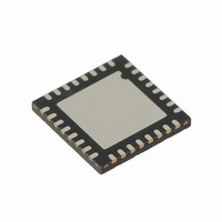
CY8CTMG200-32LQXI Cypress Semiconductor Corp, CY8CTMG200-32LQXI Datasheet - Page 136

CY8CTMG200-32LQXI
Manufacturer Part Number
CY8CTMG200-32LQXI
Description
IC MCU 32K FLASH 32UQFN
Manufacturer
Cypress Semiconductor Corp
Series
TrueTouch™r
Datasheet
1.CY8CTST200-16LGXI.pdf
(308 pages)
Specifications of CY8CTMG200-32LQXI
Program Memory Type
FLASH (32 kB)
Package / Case
32-UQFN Exposed Pad, 32-HUQFN, 32-SQFN
Applications
Touchscreen Controller
Core Processor
M8C
Controller Series
CY8CT
Ram Size
2K x 8
Interface
I²C, SPI, UART/USART, USB
Number Of I /o
28
Voltage - Supply
1.8 V
Operating Temperature
-40°C ~ 85°C
Mounting Type
Surface Mount
Processor Series
CY8CTxx2xx
Core
M8C
Data Bus Width
8 bit
Data Ram Size
2 KB
Interface Type
I2C, SPI
Maximum Clock Frequency
24 MHz
Number Of Timers
3
Operating Supply Voltage
1.71 V to 5.5 V
Mounting Style
SMD/SMT
Program Memory Size
32 KB
Lead Free Status / RoHS Status
Lead free / RoHS Compliant
For Use With
770-1000 - ISP 4PORT FOR CYPRESS PSOC MCU
Lead Free Status / Rohs Status
Lead free / RoHS Compliant
Other names
428-2954
Available stocks
Company
Part Number
Manufacturer
Quantity
Price
Company:
Part Number:
CY8CTMG200-32LQXI
Manufacturer:
CYPRESS
Quantity:
921
Company:
Part Number:
CY8CTMG200-32LQXIT
Manufacturer:
AD
Quantity:
15 186
- Current page: 136 of 308
- Download datasheet (3Mb)
16.2.2
The device’s core runs on chip regulated supply, so there is
a time delay in powering up the core. A short XRES pulse at
power up causes an external reset startup behavior. How-
ever, the event is latched and applied only after the core has
powered up (a delay of about 1 ms).
System Resets
136
Powerup External Reset Behavior
PSoC CY8CTMG20x and CY8CTST200 TRM, Document No. 001-53603 Rev. *C
16.2.3
During External Reset (XRES=1), both P1[0] and P1[1] drive
resistive low (0). After XRES deasserts, these pins continue
to drive resistive low for another eight sleep clock cycles
(approximately 200 μ s). After this time, both pins transition
to a high impedance state and normal CPU operation
begins. This is illustrated in
Figure 16-2. P1[1:0] Behavior on External Reset (XRES)
XRES
P1[0]
P1[1]
GPIO Behavior on External Reset
R0
R0
T1 = 8 Sleep Clock Cycles
T1
(approximately 200 μs)
Figure
16-2.
HiZ
HiZ
[+] Feedback
Related parts for CY8CTMG200-32LQXI
Image
Part Number
Description
Manufacturer
Datasheet
Request
R
Part Number:
Description:
CY8CTMG200-32LQXIT
Manufacturer:
Cypress Semiconductor Corp
Datasheet:

Part Number:
Description:
IC MCU 32K FLASH 16-COL
Manufacturer:
Cypress Semiconductor Corp
Datasheet:

Part Number:
Description:
IC MCU 32K FLASH 24UQFN
Manufacturer:
Cypress Semiconductor Corp
Datasheet:

Part Number:
Description:
IC MCU 32K FLASH 48-QFN
Manufacturer:
Cypress Semiconductor Corp
Datasheet:
Part Number:
Description:
IC MCU 32K FLASH 16-COL
Manufacturer:
Cypress Semiconductor Corp
Datasheet:
Part Number:
Description:
IC MCU 32K FLASH 24UQFN
Manufacturer:
Cypress Semiconductor Corp
Datasheet:
Part Number:
Description:
IC MCU 32K FLASH 48-QFN
Manufacturer:
Cypress Semiconductor Corp
Datasheet:
Part Number:
Description:
Manufacturer:
Cypress Semiconductor Corp
Datasheet:
Part Number:
Description:
Manufacturer:
Cypress Semiconductor Corp
Datasheet:


