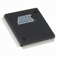
AT94K05AL-25DQC Atmel, AT94K05AL-25DQC Datasheet - Page 95

AT94K05AL-25DQC
Manufacturer Part Number
AT94K05AL-25DQC
Description
IC FPSLIC 5K GATE 25MHZ 208PQFP
Manufacturer
Atmel
Series
FPSLIC®r
Specifications of AT94K05AL-25DQC
Core Type
8-bit AVR
Speed
25MHz
Interface
I²C, UART
Program Sram Bytes
4K-16K
Fpga Sram
2kb
Data Sram Bytes
4K ~ 16K
Fpga Core Cells
256
Fpga Gates
5K
Fpga Registers
436
Voltage - Supply
3 V ~ 3.6 V
Mounting Type
Surface Mount
Operating Temperature
0°C ~ 70°C
Package / Case
208-MQFP, 208-PQFP
For Use With
ATSTK594 - BOARD FPSLIC DAUGHTER FOR STK500
Lead Free Status / RoHS Status
Contains lead / RoHS non-compliant
Eeprom Size
-
Available stocks
Company
Part Number
Manufacturer
Quantity
Price
- Current page: 95 of 204
- Download datasheet (4Mb)
4.25.1
4.25.2
1138I–FPSLI–1/08
Timer/Counter 0 and 2 in PWM Mode
PWM Modes (Up/Down and Overflow)
Both Timer/Counters are realized as up or up/down (in PWM mode) counters with read and write
access. If the Timer/Counter is written to and a clock source is selected, it continues counting in
the timer clock cycle following the write operation.
Timer/Counter0 Output Compare Register – OCR0
Timer/Counter2 Output Compare Register – OCR2
The output compare registers are 8-bit read/write registers. The Timer/Counter Output Compare
Registers contains the data to be continuously compared with the Timer/Counter. Actions on
compare matches are specified in TCCR0 and TCCR2. A compare match does only occur if the
Timer/Counter counts to the OCR value. A software write that sets Timer/Counter and Output
Compare Register to the same value does not generate a compare match.
A compare match will set the compare interrupt flag in the CPU clock-cycle following the com-
pare event.
When PWM mode is selected, the Timer/Counter either wraps (overflows) when it reaches $FF
or it acts as an up/down counter.
If the up/down mode is selected, the Timer/Counter and the Output Compare Registers – OCR0
or OCR2 form an 8-bit, free-running, glitch-free and phase correct PWM with outputs on the
PE1(OC0/PWM0) or PE3(OC2/PWM2) pin.
If the overflow mode is selected, the Timer/Counter and the Output Compare Registers – OCR0
or OCR2 form an 8-bit, free-running and glitch-free PWM, operating with twice the speed of the
up/down counting mode.
The two different PWM modes are selected by the CTC0 or CTC2 bit in the Timer/Counter Con-
trol Registers – TCCR0 or TCCR2 respectively.
If CTC0/CTC2 is cleared and PWM mode is selected, the Timer/Counter acts as an up/down
counter, counting up from $00 to $FF, where it turns and counts down again to zero before the
cycle is repeated. When the counter value matches the contents of the Output Compare Regis-
ter, the PE1(OC0/PWM0) or PE3(OC2/PWM2) pin is set or cleared according to the settings of
the COMn1/COMn0 bits in the Timer/Counter Control Registers TCCR0 or TCCR2.
If CTC0/CTC2 is set and PWM mode is selected, the Timer/Counters will wrap and start count-
ing from $00 after reaching $FF. The PE1(OC0/PWM0) or PE3(OC2/PWM2) pin will be set or
cleared according to the settings of COMn1/COMn0 on a Timer/Counter overflow or when the
counter value matches the contents of the Output Compare Register. Refer to
details.
Bit
$31 ($51)
Read/Write
Initial Value
Bit
$22 ($42)
Read/Write
Initial Value
7
MSB
R/W
0
7
MSB
R/W
0
6
R/W
0
6
R/W
0
5
0
5
0
R/W
R/W
4
R/W
0
4
R/W
0
AT94KAL Series FPSLIC
3
R/W
0
3
R/W
0
2
R/W
0
2
R/W
0
1
R/W
0
1
R/W
0
0
LSB
R/W
0
0
LSB
R/W
0
Table 4-15
OCR0
OCR2
for
95
Related parts for AT94K05AL-25DQC
Image
Part Number
Description
Manufacturer
Datasheet
Request
R

Part Number:
Description:
IC FPSLIC 5K GATE 25MHZ 84PLCC
Manufacturer:
Atmel
Datasheet:

Part Number:
Description:
Fpslic Devices Combine 5K Gates of Atmel's Patented AT40K Fpga Architecture, a 20 Mips Avr 8-bit Risc Microprocessor Core, Numerous Fixed Microcontroller Peripheries And up to 36K Bytes of Program And Data SRAM.
Manufacturer:
ATMEL Corporation
Datasheet:

Part Number:
Description:
IC FPSLIC 5K GATE 25MHZ 84PLCC
Manufacturer:
Atmel
Datasheet:

Part Number:
Description:
IC FPSLIC 5K GATE 25MHZ 144LQFP
Manufacturer:
Atmel
Datasheet:

Part Number:
Description:
IC FPSLIC 5K GATE 25MHZ 208PQFP
Manufacturer:
Atmel
Datasheet:

Part Number:
Description:
IC FPSLIC 5K GATE 25MHZ 144LQFP
Manufacturer:
Atmel
Datasheet:

Part Number:
Description:
IC FPSLIC 5K GATE 25MHZ 144-LQFP
Manufacturer:
Atmel
Datasheet:

Part Number:
Description:
IC FPSLIC 5K GATE 25MHZ 100-TQFP
Manufacturer:
Atmel
Datasheet:

Part Number:
Description:
Manufacturer:
Atmel
Datasheet:

Part Number:
Description:
Manufacturer:
Atmel
Datasheet:

Part Number:
Description:
Manufacturer:
Atmel
Datasheet:

Part Number:
Description:
5k - 40k Gates Of At40k Fpga With 8-bit Microcontroller, Up To 36k Bytes Of Sram And On-chip Jtag Ice
Manufacturer:
ATMEL Corporation
Datasheet:

Part Number:
Description:
At94k05al 5k - 40k Gates Of At40k Fpga With 8-bit Microcontroller, Up To 36k Bytes Of Sram And On-chip Jtag Ice
Manufacturer:
ATMEL Corporation
Datasheet:

Part Number:
Description:
DEV KIT FOR AVR/AVR32
Manufacturer:
Atmel
Datasheet:


