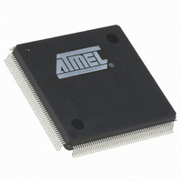
AT94K05AL-25DQC Atmel, AT94K05AL-25DQC Datasheet - Page 11

AT94K05AL-25DQC
Manufacturer Part Number
AT94K05AL-25DQC
Description
IC FPSLIC 5K GATE 25MHZ 208PQFP
Manufacturer
Atmel
Series
FPSLIC®r
Specifications of AT94K05AL-25DQC
Core Type
8-bit AVR
Speed
25MHz
Interface
I²C, UART
Program Sram Bytes
4K-16K
Fpga Sram
2kb
Data Sram Bytes
4K ~ 16K
Fpga Core Cells
256
Fpga Gates
5K
Fpga Registers
436
Voltage - Supply
3 V ~ 3.6 V
Mounting Type
Surface Mount
Operating Temperature
0°C ~ 70°C
Package / Case
208-MQFP, 208-PQFP
For Use With
ATSTK594 - BOARD FPSLIC DAUGHTER FOR STK500
Lead Free Status / RoHS Status
Contains lead / RoHS non-compliant
Eeprom Size
-
Available stocks
Company
Part Number
Manufacturer
Quantity
Price
- Current page: 11 of 204
- Download datasheet (4Mb)
1138I–FPSLI–1/08
tions in horizontally aligned RAM blocks. For the left-most RAM blocks, RAddr is on the left and
WAddr is on the right. For the right-most RAM blocks, WAddr is on the left and RAddr is tied off.
For single-ported RAM, WAddr is the READ/WRITE address port and Din is the (bi-directional)
data port. The right-most RAM blocks can be used only for single-ported memories. WE and OE
connect to the vertical express buses in the same column on Plane V
WAddr, RAddr, WE and OE connect to express buses that are full length at array edge.
Reading and writing the 32 x 4 dual-port RAM are independent of each other. Reading the
32 x 4 dual-port RAM is completely asynchronous. Latches are transparent; when Load is logic
1, data flows through; when Load is logic 0, data is latched. Each bit in the 32 x 4 dual-port RAM
is also a transparent latch. The front-end latch and the memory latch together and form an edge-
triggered flip-flop. When a bit nibble is (Write) addressed and LOAD is logic 1 and WE is logic 0,
DATA flows through the bit. When a nibble is not (Write) addressed or LOAD is logic 0 or WE is
logic 1, DATA is latched in the nibble. The two CLOCK muxes are controlled together; they both
select CLOCK or they both select “1”. CLOCK is obtained from the clock for the sector-column
immediately to the left and immediately above the RAM block. Writing any value to the RAM
Clear Byte during configuration clears the RAM, see
Figure
Figure 2-6.
2-4.
FPGA RAM Connections (One RAM Block)
AT94KAL Series FPSLIC
Figure 2-3
and
CLK
CLK
CLK
CLK
CLK
WAddr
WE
OE
1
32X4 RAM
Din
Sector Clock Mux
and V
Dout
RAddr
2
, respectively.
11
Related parts for AT94K05AL-25DQC
Image
Part Number
Description
Manufacturer
Datasheet
Request
R

Part Number:
Description:
IC FPSLIC 5K GATE 25MHZ 84PLCC
Manufacturer:
Atmel
Datasheet:

Part Number:
Description:
Fpslic Devices Combine 5K Gates of Atmel's Patented AT40K Fpga Architecture, a 20 Mips Avr 8-bit Risc Microprocessor Core, Numerous Fixed Microcontroller Peripheries And up to 36K Bytes of Program And Data SRAM.
Manufacturer:
ATMEL Corporation
Datasheet:

Part Number:
Description:
IC FPSLIC 5K GATE 25MHZ 84PLCC
Manufacturer:
Atmel
Datasheet:

Part Number:
Description:
IC FPSLIC 5K GATE 25MHZ 144LQFP
Manufacturer:
Atmel
Datasheet:

Part Number:
Description:
IC FPSLIC 5K GATE 25MHZ 208PQFP
Manufacturer:
Atmel
Datasheet:

Part Number:
Description:
IC FPSLIC 5K GATE 25MHZ 144LQFP
Manufacturer:
Atmel
Datasheet:

Part Number:
Description:
IC FPSLIC 5K GATE 25MHZ 144-LQFP
Manufacturer:
Atmel
Datasheet:

Part Number:
Description:
IC FPSLIC 5K GATE 25MHZ 100-TQFP
Manufacturer:
Atmel
Datasheet:

Part Number:
Description:
Manufacturer:
Atmel
Datasheet:

Part Number:
Description:
Manufacturer:
Atmel
Datasheet:

Part Number:
Description:
Manufacturer:
Atmel
Datasheet:

Part Number:
Description:
5k - 40k Gates Of At40k Fpga With 8-bit Microcontroller, Up To 36k Bytes Of Sram And On-chip Jtag Ice
Manufacturer:
ATMEL Corporation
Datasheet:

Part Number:
Description:
At94k05al 5k - 40k Gates Of At40k Fpga With 8-bit Microcontroller, Up To 36k Bytes Of Sram And On-chip Jtag Ice
Manufacturer:
ATMEL Corporation
Datasheet:

Part Number:
Description:
DEV KIT FOR AVR/AVR32
Manufacturer:
Atmel
Datasheet:


