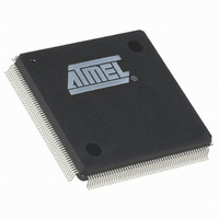
AT94K05AL-25DQC Atmel, AT94K05AL-25DQC Datasheet - Page 22

AT94K05AL-25DQC
Manufacturer Part Number
AT94K05AL-25DQC
Description
IC FPSLIC 5K GATE 25MHZ 208PQFP
Manufacturer
Atmel
Series
FPSLIC®r
Specifications of AT94K05AL-25DQC
Core Type
8-bit AVR
Speed
25MHz
Interface
I²C, UART
Program Sram Bytes
4K-16K
Fpga Sram
2kb
Data Sram Bytes
4K ~ 16K
Fpga Core Cells
256
Fpga Gates
5K
Fpga Registers
436
Voltage - Supply
3 V ~ 3.6 V
Mounting Type
Surface Mount
Operating Temperature
0°C ~ 70°C
Package / Case
208-MQFP, 208-PQFP
For Use With
ATSTK594 - BOARD FPSLIC DAUGHTER FOR STK500
Lead Free Status / RoHS Status
Contains lead / RoHS non-compliant
Eeprom Size
-
Available stocks
Company
Part Number
Manufacturer
Quantity
Price
- Current page: 22 of 204
- Download datasheet (4Mb)
3.2
Program and Data SRAM
Up to 36 Kbytes of 15 ns dual-port SRAM reside between the FPGA and the AVR. This SRAM is
used by the AVR for program instruction and general-purpose data storage. The AVR is con-
nected to one side of this SRAM; the FPGA is connected to the other side. The port connected
to the FPGA is used to store data without using up bandwidth on the AVR system data bus.
(1)
The FPGA core communicates directly with the data SRAM
block, viewing all SRAM memory
space as 8-bit memory.
Note:
1. The unused bits for the FPGA-SRAM address must tie to ‘0’ because there is no pull-down
circuitry.
For the AT94K10 and AT94K40, the internal program and data SRAM is divided into three
blocks: 10 Kbytes x 16 dedicated program SRAM, 4 Kbytes x 8 dedicated data SRAM and 6
Kbytes x 16 or 12 Kbytes x 8 configurable SRAM, which may be swapped between program and
data memory spaces in 2 Kbytes x 16 or 4 Kbytes x 8 partitions.
For the AT94K05, the internal program and data SRAM is divided into three blocks: 4 Kbytes 16
dedicated program SRAM, 4 Kbytes x 8 dedicated data SRAM and 6 Kbytes x 16 or 12
Kbytes x 8 configurable SRAM, which may be swapped between program and data memory
spaces in 2 Kbytes x 16 or 4 Kbytes x 8 partitions.
The addressing scheme for the configurable SRAM partitions prevents program instructions
from overwriting data words and vice versa. Once configured (SCR41:40 –
See “System Control
Register – FPGA/AVR” on page
30.), the program memory space remains isolated from the data
memory space. SCR41:40 controls internal muxes. Write enable signals allow the memory to be
safely segmented.
Figure 3-2
shows the FPSLIC configurable allocation SRAM memory.
AT94KAL Series FPSLIC
22
1138I–FPSLI–1/08
Related parts for AT94K05AL-25DQC
Image
Part Number
Description
Manufacturer
Datasheet
Request
R

Part Number:
Description:
IC FPSLIC 5K GATE 25MHZ 84PLCC
Manufacturer:
Atmel
Datasheet:

Part Number:
Description:
Fpslic Devices Combine 5K Gates of Atmel's Patented AT40K Fpga Architecture, a 20 Mips Avr 8-bit Risc Microprocessor Core, Numerous Fixed Microcontroller Peripheries And up to 36K Bytes of Program And Data SRAM.
Manufacturer:
ATMEL Corporation
Datasheet:

Part Number:
Description:
IC FPSLIC 5K GATE 25MHZ 84PLCC
Manufacturer:
Atmel
Datasheet:

Part Number:
Description:
IC FPSLIC 5K GATE 25MHZ 144LQFP
Manufacturer:
Atmel
Datasheet:

Part Number:
Description:
IC FPSLIC 5K GATE 25MHZ 208PQFP
Manufacturer:
Atmel
Datasheet:

Part Number:
Description:
IC FPSLIC 5K GATE 25MHZ 144LQFP
Manufacturer:
Atmel
Datasheet:

Part Number:
Description:
IC FPSLIC 5K GATE 25MHZ 144-LQFP
Manufacturer:
Atmel
Datasheet:

Part Number:
Description:
IC FPSLIC 5K GATE 25MHZ 100-TQFP
Manufacturer:
Atmel
Datasheet:

Part Number:
Description:
Manufacturer:
Atmel
Datasheet:

Part Number:
Description:
Manufacturer:
Atmel
Datasheet:

Part Number:
Description:
Manufacturer:
Atmel
Datasheet:

Part Number:
Description:
5k - 40k Gates Of At40k Fpga With 8-bit Microcontroller, Up To 36k Bytes Of Sram And On-chip Jtag Ice
Manufacturer:
ATMEL Corporation
Datasheet:

Part Number:
Description:
At94k05al 5k - 40k Gates Of At40k Fpga With 8-bit Microcontroller, Up To 36k Bytes Of Sram And On-chip Jtag Ice
Manufacturer:
ATMEL Corporation
Datasheet:

Part Number:
Description:
DEV KIT FOR AVR/AVR32
Manufacturer:
Atmel
Datasheet:


