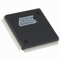
AT94K05AL-25DQC Atmel, AT94K05AL-25DQC Datasheet - Page 180

AT94K05AL-25DQC
Manufacturer Part Number
AT94K05AL-25DQC
Description
IC FPSLIC 5K GATE 25MHZ 208PQFP
Manufacturer
Atmel
Series
FPSLIC®r
Specifications of AT94K05AL-25DQC
Core Type
8-bit AVR
Speed
25MHz
Interface
I²C, UART
Program Sram Bytes
4K-16K
Fpga Sram
2kb
Data Sram Bytes
4K ~ 16K
Fpga Core Cells
256
Fpga Gates
5K
Fpga Registers
436
Voltage - Supply
3 V ~ 3.6 V
Mounting Type
Surface Mount
Operating Temperature
0°C ~ 70°C
Package / Case
208-MQFP, 208-PQFP
For Use With
ATSTK594 - BOARD FPSLIC DAUGHTER FOR STK500
Lead Free Status / RoHS Status
Contains lead / RoHS non-compliant
Eeprom Size
-
Available stocks
Company
Part Number
Manufacturer
Quantity
Price
- Current page: 180 of 204
- Download datasheet (4Mb)
6.6
CMOS buffer delays are measured from a V
stant. Buffer delay is to a pad voltage of 1.5V with one output switching. Parameter based on characterization and
simulation; not tested in production. An FPGA power calculation is available in Atmel’s System Designer software (see also
page
180
Cell Function
Async RAM
Write
Write
Write
Write
Write
Write
Write
Write
Write/Read
Read
Read
Read
Sync RAM
Write
Write
Write
Write
Write
Write
Write
Write
Write
Write/Read
Write/Read
Read
Read
Read
171).
AC Timing Characteristics – 3.3V Operation
Delays are based on fixed loads and are described in the notes.
Maximum times based on worst case: V
Minimum times based on best case: V
AT94KAL Series FPSLIC
Parameter
t
t
t
t
t
t
t
t
t
t
t
t
t
t
t
t
t
t
t
t
t
t
t
t
t
t
WECYC
WEL
WEH
setup
hold
setup
hold
hold
PD
PD
PZX
PXZ
CYC
CLKL
CLKH
setup
hold
setup
hold
setup
hold
PD
PD
PD
PZX
PXZ
(Maximum)
(Maximum)
(Maximum)
(Maximum)
(Maximum)
(Minimum)
(Minimum)
(Minimum)
(Maximum)
(Maximum)
(Minimum)
(Minimum)
(Minimum)
(Maximum)
(Maximum)
(Minimum)
(Minimum)
(Minimum)
(Minimum)
(Minimum)
(Minimum)
(Minimum)
(Minimum)
(Minimum)
(Minimum)
(Minimum)
CC
CC
= 3.6V, temperature = 0° C
IH
= 3.0V, temperature = 70° C
Path
cycle time
we
we
wr addr setup-> we
wr addr hold -> we
din setup -> we
din hold -> we
oe hold -> we
din -> dout
rd addr -> dout
oe -> dout
oe -> dout
cycle time
clk
clk
we setup-> clk
we hold -> clk
wr addr setup-> clk
wr addr hold -> clk
wr data setup-> clk
wr data hold -> clk
din -> dout
clk -> dout
rd addr -> dout
oe -> dout
oe -> dout
of 1/2 V
CC
at the pad to the internal V
12.0
12.0
-25
5.0
5.0
5.3
0.0
5.0
0.0
0.0
8.7
6.3
2.9
3.5
5.0
5.0
3.2
0.0
5.0
0.0
3.9
0.0
8.7
5.8
6.3
2.9
3.5
IH
Units
at A. The input buffer load is con-
ns
ns
ns
ns
ns
ns
ns
ns
ns
ns
ns
ns
ns
ns
ns
ns
ns
ns
ns
ns
ns
ns
ns
ns
ns
ns
Notes
–
Pulse Width Low
Pulse Width High
–
–
rd addr = wr addr
–
–
Pulse Width High
–
–
–
rd addr = wr addr
rd addr = wr addr
–
1138I–FPSLI–1/08
Related parts for AT94K05AL-25DQC
Image
Part Number
Description
Manufacturer
Datasheet
Request
R

Part Number:
Description:
IC FPSLIC 5K GATE 25MHZ 84PLCC
Manufacturer:
Atmel
Datasheet:

Part Number:
Description:
Fpslic Devices Combine 5K Gates of Atmel's Patented AT40K Fpga Architecture, a 20 Mips Avr 8-bit Risc Microprocessor Core, Numerous Fixed Microcontroller Peripheries And up to 36K Bytes of Program And Data SRAM.
Manufacturer:
ATMEL Corporation
Datasheet:

Part Number:
Description:
IC FPSLIC 5K GATE 25MHZ 84PLCC
Manufacturer:
Atmel
Datasheet:

Part Number:
Description:
IC FPSLIC 5K GATE 25MHZ 144LQFP
Manufacturer:
Atmel
Datasheet:

Part Number:
Description:
IC FPSLIC 5K GATE 25MHZ 208PQFP
Manufacturer:
Atmel
Datasheet:

Part Number:
Description:
IC FPSLIC 5K GATE 25MHZ 144LQFP
Manufacturer:
Atmel
Datasheet:

Part Number:
Description:
IC FPSLIC 5K GATE 25MHZ 144-LQFP
Manufacturer:
Atmel
Datasheet:

Part Number:
Description:
IC FPSLIC 5K GATE 25MHZ 100-TQFP
Manufacturer:
Atmel
Datasheet:

Part Number:
Description:
Manufacturer:
Atmel
Datasheet:

Part Number:
Description:
Manufacturer:
Atmel
Datasheet:

Part Number:
Description:
Manufacturer:
Atmel
Datasheet:

Part Number:
Description:
5k - 40k Gates Of At40k Fpga With 8-bit Microcontroller, Up To 36k Bytes Of Sram And On-chip Jtag Ice
Manufacturer:
ATMEL Corporation
Datasheet:

Part Number:
Description:
At94k05al 5k - 40k Gates Of At40k Fpga With 8-bit Microcontroller, Up To 36k Bytes Of Sram And On-chip Jtag Ice
Manufacturer:
ATMEL Corporation
Datasheet:

Part Number:
Description:
DEV KIT FOR AVR/AVR32
Manufacturer:
Atmel
Datasheet:


