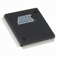
AT94K05AL-25DQC Atmel, AT94K05AL-25DQC Datasheet - Page 132

AT94K05AL-25DQC
Manufacturer Part Number
AT94K05AL-25DQC
Description
IC FPSLIC 5K GATE 25MHZ 208PQFP
Manufacturer
Atmel
Series
FPSLIC®r
Specifications of AT94K05AL-25DQC
Core Type
8-bit AVR
Speed
25MHz
Interface
I²C, UART
Program Sram Bytes
4K-16K
Fpga Sram
2kb
Data Sram Bytes
4K ~ 16K
Fpga Core Cells
256
Fpga Gates
5K
Fpga Registers
436
Voltage - Supply
3 V ~ 3.6 V
Mounting Type
Surface Mount
Operating Temperature
0°C ~ 70°C
Package / Case
208-MQFP, 208-PQFP
For Use With
ATSTK594 - BOARD FPSLIC DAUGHTER FOR STK500
Lead Free Status / RoHS Status
Contains lead / RoHS non-compliant
Eeprom Size
-
Available stocks
Company
Part Number
Manufacturer
Quantity
Price
- Current page: 132 of 204
- Download datasheet (4Mb)
If however, a valid start bit is detected, sampling of the data bits following the start bit is per-
formed. These bits are also sampled at samples 8, 9 and 10. The logical value found in at least
two of the three samples is taken as the bit value. All bits are shifted into the transmitter shift reg-
ister as they are sampled. Sampling of an incoming character is shown in
Figure
4-43. Note that
the description above is not valid when the UART transmission speed is doubled. See
“Double
Speed Transmission” on page 138
for a detailed description.
(1)
Figure 4-43. Sampling Received Data
“Double Speed Transmis-
Note:
1. This figure is not valid when the UART speed is doubled. See
sion” on page 138
for a detailed description.
When the stop bit enters the receiver, the majority of the three samples must be one to accept
the stop bit. If two or more samples are logic 0s, the Framing Error (FEn) flag in the UART Con-
trol and Status Register (UCSRnA) is set. Before reading the UDRn register, the user should
always check the FEn bit to detect Framing Errors.
Whether or not a valid stop bit is detected at the end of a character reception cycle, the data is
transferred to UDRn and the RXCn flag in UCSRnA is set. UDRn is in fact two physically sepa-
rate registers, one for transmitted data and one for received data. When UDRn is read, the
Receive Data register is accessed, and when UDRn is written, the Transmit Data register is
accessed. If the 9-bit data word is selected (the CHR9n bit in the UART Control and Status Reg-
ister, UCSRnB is set), the RXB8n bit in UCSRnB is loaded with bit 9 in the Transmit shift register
when data is transferred to UDRn.
If, after having received a character, the UDRn register has not been read since the last receive,
the OverRun (ORn) flag in UCSRnB is set. This means that the last data byte shifted into to the
shift register could not be transferred to UDRn and has been lost. The ORn bit is buffered, and is
updated when the valid data byte in UDRn is read. Thus, the user should always check the ORn
bit after reading the UDRn register in order to detect any overruns if the baud-rate is High or
CPU load is High.
When the RXEN bit in the UCSRnB register is cleared (zero), the receiver is disabled. This
means that the PE1 (n=0) or PE3 (n=1) pin can be used as a general I/O pin. When RXEN
is
n
set, the UART Receiver will be connected to PE1 (UART0) or PE3 (UART1), which is forced to
be an input pin regardless of the setting of the DDE1 in DDRE (UART0) or DDB2 bit in DDRB
(UART1). When PE1 (UART0) or PE3 (UART1) is forced to input by the UART, the PORTE1
(UART0) or PORTE3 (UART1) bit can still be used to control the pull-up resistor on the pin.
When the CHR9n bit in the UCSRnB register is set, transmitted and received characters are 9
bits long plus start and stop bits. The 9th data bit to be transmitted is the TXB8n bit in UCSRnB
register. This bit must be set to the wanted value before a transmission is initiated by writing to
the UDRn register. The 9th data bit received is the RXB8n bit in the UCSRnB register.
AT94KAL Series FPSLIC
132
1138I–FPSLI–1/08
Related parts for AT94K05AL-25DQC
Image
Part Number
Description
Manufacturer
Datasheet
Request
R

Part Number:
Description:
IC FPSLIC 5K GATE 25MHZ 84PLCC
Manufacturer:
Atmel
Datasheet:

Part Number:
Description:
Fpslic Devices Combine 5K Gates of Atmel's Patented AT40K Fpga Architecture, a 20 Mips Avr 8-bit Risc Microprocessor Core, Numerous Fixed Microcontroller Peripheries And up to 36K Bytes of Program And Data SRAM.
Manufacturer:
ATMEL Corporation
Datasheet:

Part Number:
Description:
IC FPSLIC 5K GATE 25MHZ 84PLCC
Manufacturer:
Atmel
Datasheet:

Part Number:
Description:
IC FPSLIC 5K GATE 25MHZ 144LQFP
Manufacturer:
Atmel
Datasheet:

Part Number:
Description:
IC FPSLIC 5K GATE 25MHZ 208PQFP
Manufacturer:
Atmel
Datasheet:

Part Number:
Description:
IC FPSLIC 5K GATE 25MHZ 144LQFP
Manufacturer:
Atmel
Datasheet:

Part Number:
Description:
IC FPSLIC 5K GATE 25MHZ 144-LQFP
Manufacturer:
Atmel
Datasheet:

Part Number:
Description:
IC FPSLIC 5K GATE 25MHZ 100-TQFP
Manufacturer:
Atmel
Datasheet:

Part Number:
Description:
Manufacturer:
Atmel
Datasheet:

Part Number:
Description:
Manufacturer:
Atmel
Datasheet:

Part Number:
Description:
Manufacturer:
Atmel
Datasheet:

Part Number:
Description:
5k - 40k Gates Of At40k Fpga With 8-bit Microcontroller, Up To 36k Bytes Of Sram And On-chip Jtag Ice
Manufacturer:
ATMEL Corporation
Datasheet:

Part Number:
Description:
At94k05al 5k - 40k Gates Of At40k Fpga With 8-bit Microcontroller, Up To 36k Bytes Of Sram And On-chip Jtag Ice
Manufacturer:
ATMEL Corporation
Datasheet:

Part Number:
Description:
DEV KIT FOR AVR/AVR32
Manufacturer:
Atmel
Datasheet:


