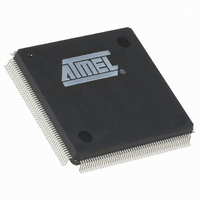
AT94K05AL-25DQC Atmel, AT94K05AL-25DQC Datasheet - Page 53

AT94K05AL-25DQC
Manufacturer Part Number
AT94K05AL-25DQC
Description
IC FPSLIC 5K GATE 25MHZ 208PQFP
Manufacturer
Atmel
Series
FPSLIC®r
Specifications of AT94K05AL-25DQC
Core Type
8-bit AVR
Speed
25MHz
Interface
I²C, UART
Program Sram Bytes
4K-16K
Fpga Sram
2kb
Data Sram Bytes
4K ~ 16K
Fpga Core Cells
256
Fpga Gates
5K
Fpga Registers
436
Voltage - Supply
3 V ~ 3.6 V
Mounting Type
Surface Mount
Operating Temperature
0°C ~ 70°C
Package / Case
208-MQFP, 208-PQFP
For Use With
ATSTK594 - BOARD FPSLIC DAUGHTER FOR STK500
Lead Free Status / RoHS Status
Contains lead / RoHS non-compliant
Eeprom Size
-
Available stocks
Company
Part Number
Manufacturer
Quantity
Price
- Current page: 53 of 204
- Download datasheet (4Mb)
1138I–FPSLI–1/08
When this bit is set to 1, the AVR can write its own program SRAM. During AVR reset, the DBG
bit is cleared by the hardware.
• Bit 0 - SRST: Software Reset
When this bit is set (one), a reset request is sent to the system configuration external to the
AVR. Appropriate reset signals are generated back into the AVR and configuration download is
initiated. A software reset will cause the EXTRF bit in the MCUR register to be set (one), which
remains set throughout the AVR reset and may be read by the restarted program upon reset
complete. The external reset flag is set (one) since the requested reset is issued from the sys-
tem configuration external to the AVR core. During AVR reset, the SRST bit is cleared by the
hardware.
MCU Control Status/Register – MCUR
The MCU Register contains control bits for general MCU functions and status bits to indicate the
source of an MCU reset.
• Bit 7 - JTRF: JTAG Reset Flag
This flag is set (one) upon issuing the AVR_RESET ($C) JTAG instruction. The flag can only be
cleared (zero) by writing a zero to the JTRF bit or by a power-on reset. The bit will not be cleared
by hardware during AVR reset.
• Bit 6 - JTD: JTAG Disable
When this bit is cleared (zero), and the System Control Register JTAG Enable bit is set (one),
the JTAG interface is disabled. To avoid unintentional disabling or enabling of the JTAG inter-
face, a timed sequence must be followed when changing this bit: the application software must
write this bit to the desired value twice within four cycles to change its value.
• Bit 5 - SE: Sleep Enable
The SE bit must be set (one) to make the MCU enter the Sleep mode when the SLEEP instruc-
tion is executed. To avoid the MCU entering the Sleep mode unless it is the programmers
purpose, it is recommended to set the Sleep Enable SE bit just before the execution of the
SLEEP instruction.
• Bits 4, 3 - SM1/SM0: Sleep Mode Select Bits 1 and 0
This bit selects between the three available Sleep modes as shown in
• Bit 2 - PORF: Power-on Reset Flag
This flag is set (one) upon power-up of the device. The flag can only be cleared (zero) by writing
a zero to the PORF bit. The bit will not be cleared by the hardware during AVR reset.
• Bit 1 - WDRF: Watchdog Reset Flag
This bit is set if a watchdog reset occurs. The bit is cleared by writing a logic 0 to the flag.
Bit
$35 ($55)
Read/Write
Initial Value
7
JTRF
R/W
0
6
JTD
R/W
0
5
SE
R/W
0
4
SM1
R/W
0
AT94KAL Series FPSLIC
3
SM0
R/W
0
2
PORF
R/W
1
1
WDRF
R/W
0
Table
4-3.
0
EXTRF
R/W
1
MCUR
53
Related parts for AT94K05AL-25DQC
Image
Part Number
Description
Manufacturer
Datasheet
Request
R

Part Number:
Description:
IC FPSLIC 5K GATE 25MHZ 84PLCC
Manufacturer:
Atmel
Datasheet:

Part Number:
Description:
Fpslic Devices Combine 5K Gates of Atmel's Patented AT40K Fpga Architecture, a 20 Mips Avr 8-bit Risc Microprocessor Core, Numerous Fixed Microcontroller Peripheries And up to 36K Bytes of Program And Data SRAM.
Manufacturer:
ATMEL Corporation
Datasheet:

Part Number:
Description:
IC FPSLIC 5K GATE 25MHZ 84PLCC
Manufacturer:
Atmel
Datasheet:

Part Number:
Description:
IC FPSLIC 5K GATE 25MHZ 144LQFP
Manufacturer:
Atmel
Datasheet:

Part Number:
Description:
IC FPSLIC 5K GATE 25MHZ 208PQFP
Manufacturer:
Atmel
Datasheet:

Part Number:
Description:
IC FPSLIC 5K GATE 25MHZ 144LQFP
Manufacturer:
Atmel
Datasheet:

Part Number:
Description:
IC FPSLIC 5K GATE 25MHZ 144-LQFP
Manufacturer:
Atmel
Datasheet:

Part Number:
Description:
IC FPSLIC 5K GATE 25MHZ 100-TQFP
Manufacturer:
Atmel
Datasheet:

Part Number:
Description:
Manufacturer:
Atmel
Datasheet:

Part Number:
Description:
Manufacturer:
Atmel
Datasheet:

Part Number:
Description:
Manufacturer:
Atmel
Datasheet:

Part Number:
Description:
5k - 40k Gates Of At40k Fpga With 8-bit Microcontroller, Up To 36k Bytes Of Sram And On-chip Jtag Ice
Manufacturer:
ATMEL Corporation
Datasheet:

Part Number:
Description:
At94k05al 5k - 40k Gates Of At40k Fpga With 8-bit Microcontroller, Up To 36k Bytes Of Sram And On-chip Jtag Ice
Manufacturer:
ATMEL Corporation
Datasheet:

Part Number:
Description:
DEV KIT FOR AVR/AVR32
Manufacturer:
Atmel
Datasheet:


