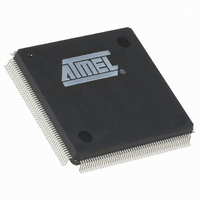
AT94K05AL-25DQC Atmel, AT94K05AL-25DQC Datasheet - Page 161

AT94K05AL-25DQC
Manufacturer Part Number
AT94K05AL-25DQC
Description
IC FPSLIC 5K GATE 25MHZ 208PQFP
Manufacturer
Atmel
Series
FPSLIC®r
Specifications of AT94K05AL-25DQC
Core Type
8-bit AVR
Speed
25MHz
Interface
I²C, UART
Program Sram Bytes
4K-16K
Fpga Sram
2kb
Data Sram Bytes
4K ~ 16K
Fpga Core Cells
256
Fpga Gates
5K
Fpga Registers
436
Voltage - Supply
3 V ~ 3.6 V
Mounting Type
Surface Mount
Operating Temperature
0°C ~ 70°C
Package / Case
208-MQFP, 208-PQFP
For Use With
ATSTK594 - BOARD FPSLIC DAUGHTER FOR STK500
Lead Free Status / RoHS Status
Contains lead / RoHS non-compliant
Eeprom Size
-
Available stocks
Company
Part Number
Manufacturer
Quantity
Price
- Current page: 161 of 204
- Download datasheet (4Mb)
4.31.2.1
4.31.2.2
1138I–FPSLI–1/08
LowPortE as General Digital I/O
Alternate Functions of PortE
PEn, General I/O pin: The DDEn bit in the DDRE register selects the direction of this pin. If
DDEn is set (one), PEn is configured as an output pin. If DDEn is cleared (zero), PEn is config-
ured as an input pin. If PEn is set (one) when configured as an input pin, the MOS pull-up
resistor is activated. To switch the pull-up resistor off the PEn has to be cleared (zero) or the pin
has to be configured as an output pin. The port pins are input with pull-up when a reset condition
becomes active, even if the clock is not running.
Table 4-36.
Note:
• PortE, Bit 0
UART0 Transmit Pin.
• PortE, Bit 1
UART0 Receive Pin. Receive Data (Data input pin for the UART0). When the UART0 receiver is
enabled this pin is configured as an input regardless of the value of DDRE0. When the UART0
forces this pin to be an input, a logic 1 in PORTE0 will turn on the internal pull-up.
• PortE, Bit 2
UART1 Transmit Pin. The alternate functions of Port E as UART0 pins are enabled by setting bit
SCR52 in the FPSLIC System Control Register. This is necessary only in smaller pinout pack-
ages where the UART signals are not bonded out. The alternate functions of Port E as UART1
pins are enabled by setting bit SCR53 in the FPSLIC System Control Register.
• PortE, Bit 3
UART1 Receive Pin. Receive Data (Data input pin for the UART1). When the UART1 receiver is
enabled this pin is configured as an input regardless of the value of DDRE2. When the UART1
forces this pin to be an input, a logic 1 in PORTE2 will turn on the internal pull-up.
• PortE, Bit 4-7
External Interrupt sources 0/1/2/3: The PE4 – PE7 pins can serve as external interrupt sources
to the MCU. Interrupts can be triggered by low-level on these pins. The internal pull-up MOS
resistors can be activated as described above.
The alternate functions of PortE as Interrupt pins by setting a bit in the System Control Register.
INT0 is controlled by SCR48. INT1 is controlled by SCR49. INT2 is controlled by SCR50. INT3 is
controlled by SCR51.
PortE, Bit 7 also shares a pin with the configuration control signal CHECK. Lowering CON to ini-
tiate an FPSLIC download (whether for loading or Checking) causes the PE7/CHECK pin to
DDEn
0
0
1
1
(1)
1. n: 7,6...0, pin number
PORTEn
DDEn
0
1
0
1
(1)
(1)
Bits on PortE Pins
Output
Output
Input
Input
I/O
Pull-up
Yes
No
No
No
AT94KAL Series FPSLIC
Comment
Tri-state (High-Z)
PDn
if external pulled Low (default).
Push-pull zero output
Push-pull one output
(1)
will source current
161
Related parts for AT94K05AL-25DQC
Image
Part Number
Description
Manufacturer
Datasheet
Request
R

Part Number:
Description:
IC FPSLIC 5K GATE 25MHZ 84PLCC
Manufacturer:
Atmel
Datasheet:

Part Number:
Description:
Fpslic Devices Combine 5K Gates of Atmel's Patented AT40K Fpga Architecture, a 20 Mips Avr 8-bit Risc Microprocessor Core, Numerous Fixed Microcontroller Peripheries And up to 36K Bytes of Program And Data SRAM.
Manufacturer:
ATMEL Corporation
Datasheet:

Part Number:
Description:
IC FPSLIC 5K GATE 25MHZ 84PLCC
Manufacturer:
Atmel
Datasheet:

Part Number:
Description:
IC FPSLIC 5K GATE 25MHZ 144LQFP
Manufacturer:
Atmel
Datasheet:

Part Number:
Description:
IC FPSLIC 5K GATE 25MHZ 208PQFP
Manufacturer:
Atmel
Datasheet:

Part Number:
Description:
IC FPSLIC 5K GATE 25MHZ 144LQFP
Manufacturer:
Atmel
Datasheet:

Part Number:
Description:
IC FPSLIC 5K GATE 25MHZ 144-LQFP
Manufacturer:
Atmel
Datasheet:

Part Number:
Description:
IC FPSLIC 5K GATE 25MHZ 100-TQFP
Manufacturer:
Atmel
Datasheet:

Part Number:
Description:
Manufacturer:
Atmel
Datasheet:

Part Number:
Description:
Manufacturer:
Atmel
Datasheet:

Part Number:
Description:
Manufacturer:
Atmel
Datasheet:

Part Number:
Description:
5k - 40k Gates Of At40k Fpga With 8-bit Microcontroller, Up To 36k Bytes Of Sram And On-chip Jtag Ice
Manufacturer:
ATMEL Corporation
Datasheet:

Part Number:
Description:
At94k05al 5k - 40k Gates Of At40k Fpga With 8-bit Microcontroller, Up To 36k Bytes Of Sram And On-chip Jtag Ice
Manufacturer:
ATMEL Corporation
Datasheet:

Part Number:
Description:
DEV KIT FOR AVR/AVR32
Manufacturer:
Atmel
Datasheet:


