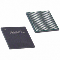
EP3C25F324I7 Altera, EP3C25F324I7 Datasheet - Page 81

EP3C25F324I7
Manufacturer Part Number
EP3C25F324I7
Description
IC CYCLONE III FPGA 25K 324 FBGA
Manufacturer
Altera
Series
Cyclone® IIIr
Datasheets
1.EP3C5F256C8N.pdf
(5 pages)
2.EP3C5F256C8N.pdf
(34 pages)
3.EP3C5F256C8N.pdf
(66 pages)
4.EP3C5F256C8N.pdf
(14 pages)
5.EP3C5F256C8N.pdf
(76 pages)
6.EP3C25F324I7.pdf
(274 pages)
Specifications of EP3C25F324I7
Number Of Logic Elements/cells
24624
Number Of Labs/clbs
1539
Total Ram Bits
608256
Number Of I /o
215
Voltage - Supply
1.15 V ~ 1.25 V
Mounting Type
Surface Mount
Operating Temperature
-40°C ~ 100°C
Package / Case
324-FBGA
Family Name
Cyclone III
Number Of Logic Blocks/elements
24624
# I/os (max)
215
Frequency (max)
437.5MHz
Process Technology
65nm
Operating Supply Voltage (typ)
1.2V
Logic Cells
24624
Ram Bits
608256
Operating Supply Voltage (min)
1.15V
Operating Supply Voltage (max)
1.25V
Operating Temp Range
-40C to 100C
Operating Temperature Classification
Industrial
Mounting
Surface Mount
Pin Count
324
Package Type
FBGA
For Use With
544-2370 - KIT STARTER CYCLONE III EP3C25
Lead Free Status / RoHS Status
Contains lead / RoHS non-compliant
Number Of Gates
-
Lead Free Status / Rohs Status
Not Compliant
Available stocks
Company
Part Number
Manufacturer
Quantity
Price
Company:
Part Number:
EP3C25F324I7N
Manufacturer:
ALTERA32
Quantity:
181
Chapter 5: Clock Networks and PLLs in the Cyclone III Device Family
Hardware Features
PLL Control Signals
© December 2009
1
1
Altera Corporation
You can use the following three signals to observe and control the PLL operation and
resynchronization.
pfdena
Use the pfdena signal to maintain the last locked frequency so that your system has
time to store its current settings before shutting down. The pfdena signal controls the
PFD output with a programmable gate. If you disable the PFD, the VCO operates at
its last set value of control voltage and frequency with some long-term drift to a lower
frequency.
areset
The areset signal is the reset or resynchronization input for each PLL. The device
input pins or internal logic can drive these input signals. When driven high, the PLL
counters reset, clearing the PLL output and placing the PLL out of lock. The VCO is
then set back to its nominal setting. When driven low again, the PLL resynchronizes
to its input as it re-locks.
You must include the areset signal in your designs if one of the following
conditions is true:
■
■
If the input clock to the PLL is toggling or unstable upon power up, assert the areset
signal after the input clock is stable and within specifications.
locked
The locked output indicates that the PLL has locked onto the reference clock and the
PLL clock outputs are operating at the desired phase and frequency set in the
Quartus II MegaWizard
Altera recommends that you use the areset and locked signals in your designs to
control and observe the status of your PLL.
This implementation is illustrated in
Figure 5–13. Locked Signal Implementation
PLL reconfiguration or clock switchover enabled in your design
Phase relationships between the PLL input clock and output clocks must be
maintained after a loss-of-lock condition
™
PLL
Plug-in Manager.
locked
Figure
V
CC
5–13.
D
OFF
Q
areset
Cyclone III Device Handbook, Volume 1
locked
5–17


