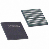
EP3C25F324I7 Altera, EP3C25F324I7 Datasheet - Page 75

EP3C25F324I7
Manufacturer Part Number
EP3C25F324I7
Description
IC CYCLONE III FPGA 25K 324 FBGA
Manufacturer
Altera
Series
Cyclone® IIIr
Datasheets
1.EP3C5F256C8N.pdf
(5 pages)
2.EP3C5F256C8N.pdf
(34 pages)
3.EP3C5F256C8N.pdf
(66 pages)
4.EP3C5F256C8N.pdf
(14 pages)
5.EP3C5F256C8N.pdf
(76 pages)
6.EP3C25F324I7.pdf
(274 pages)
Specifications of EP3C25F324I7
Number Of Logic Elements/cells
24624
Number Of Labs/clbs
1539
Total Ram Bits
608256
Number Of I /o
215
Voltage - Supply
1.15 V ~ 1.25 V
Mounting Type
Surface Mount
Operating Temperature
-40°C ~ 100°C
Package / Case
324-FBGA
Family Name
Cyclone III
Number Of Logic Blocks/elements
24624
# I/os (max)
215
Frequency (max)
437.5MHz
Process Technology
65nm
Operating Supply Voltage (typ)
1.2V
Logic Cells
24624
Ram Bits
608256
Operating Supply Voltage (min)
1.15V
Operating Supply Voltage (max)
1.25V
Operating Temp Range
-40C to 100C
Operating Temperature Classification
Industrial
Mounting
Surface Mount
Pin Count
324
Package Type
FBGA
For Use With
544-2370 - KIT STARTER CYCLONE III EP3C25
Lead Free Status / RoHS Status
Contains lead / RoHS non-compliant
Number Of Gates
-
Lead Free Status / Rohs Status
Not Compliant
Available stocks
Company
Part Number
Manufacturer
Quantity
Price
Company:
Part Number:
EP3C25F324I7N
Manufacturer:
ALTERA32
Quantity:
181
Chapter 5: Clock Networks and PLLs in the Cyclone III Device Family
Cyclone III Device Family PLL Hardware Overview
© December 2009
f
Altera Corporation
Figure 5–7
Figure 5–7. External Clock Outputs for PLLs
Notes to
(1) These external clock enable signals are available only when using the ALTCLKCTRL megafunction.
(2) PLL#_CLKOUTp and PLL#_CLKOUTn pins are dual-purpose I/O pins that you can use as one single-ended or
Each pin of a differential output pair is 180° out of phase. The Quartus II software
places the NOT gate in your design into the I/O element to implement 180° phase
with respect to the other pin in the pair. The clock output pin pairs support the same
I/O standards as standard output pins (in the top and bottom banks) as well as LVDS,
LVPECL, differential HSTL, and differential SSTL.
To determine which I/O standards are supported by the PLL clock input and output
pins, refer to the
Cyclone III device family PLLs can drive out to any regular I/O pin through the
GCLK. You can also use the external clock output pins as general purpose I/O pins if
external PLL clocking is not required.
one differential clock output.
Figure
shows the external clock outputs for PLLs.
5–7:
Cyclone III Device I/O Features
PLL #
clkena 0
C0
C1
C2
C3
C4
PLL #_CLKOUTp
(1)
chapter.
PLL #_CLKOUTn
(2)
Cyclone III Device Handbook, Volume 1
clkena 1
(2)
(1)
5–11


