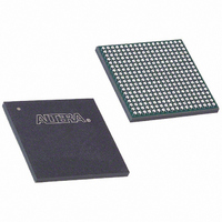
EP3C25F324I7 Altera, EP3C25F324I7 Datasheet - Page 250

EP3C25F324I7
Manufacturer Part Number
EP3C25F324I7
Description
IC CYCLONE III FPGA 25K 324 FBGA
Manufacturer
Altera
Series
Cyclone® IIIr
Datasheets
1.EP3C5F256C8N.pdf
(5 pages)
2.EP3C5F256C8N.pdf
(34 pages)
3.EP3C5F256C8N.pdf
(66 pages)
4.EP3C5F256C8N.pdf
(14 pages)
5.EP3C5F256C8N.pdf
(76 pages)
6.EP3C25F324I7.pdf
(274 pages)
Specifications of EP3C25F324I7
Number Of Logic Elements/cells
24624
Number Of Labs/clbs
1539
Total Ram Bits
608256
Number Of I /o
215
Voltage - Supply
1.15 V ~ 1.25 V
Mounting Type
Surface Mount
Operating Temperature
-40°C ~ 100°C
Package / Case
324-FBGA
Family Name
Cyclone III
Number Of Logic Blocks/elements
24624
# I/os (max)
215
Frequency (max)
437.5MHz
Process Technology
65nm
Operating Supply Voltage (typ)
1.2V
Logic Cells
24624
Ram Bits
608256
Operating Supply Voltage (min)
1.15V
Operating Supply Voltage (max)
1.25V
Operating Temp Range
-40C to 100C
Operating Temperature Classification
Industrial
Mounting
Surface Mount
Pin Count
324
Package Type
FBGA
For Use With
544-2370 - KIT STARTER CYCLONE III EP3C25
Lead Free Status / RoHS Status
Contains lead / RoHS non-compliant
Number Of Gates
-
Lead Free Status / Rohs Status
Not Compliant
Available stocks
Company
Part Number
Manufacturer
Quantity
Price
Company:
Part Number:
EP3C25F324I7N
Manufacturer:
ALTERA32
Quantity:
181
10–2
I/O Pins Remain Tristated During Power-Up
Cyclone III Device Handbook, Volume 1
f
The output buffers of Cyclone III device family are turned off during system
power up or power down. Cyclone III device family does not drive out until the
device is configured and working in recommended operating conditions. The I/O
pins are tristated until the device enters user mode with a weak pull-up resistor (R) to
V
You can power-up or power down the V
The V
The maximum power ramp rate is 3 ms for fast POR time and 50 ms for standard POR
time. The minimum power ramp rate is 50 µs. V
powered up during device operation. All V
when PLLs are not used), and must be powered up and powered down at the same
time. V
ferrite bead. During hot-socketing, the I/O pin capacitance is less than 15 pF and the
clock pin capacitance is less than 20 pF.
Cyclone III device family meets the following hot-socketing specification:
■
■
For ramp rates faster than 10 ns on I/O pins, |I
I = C dv/dt, in which C is the I/O pin capacitance and dv/dt is the slew rate. The
hot-socketing specification takes into account the pin capacitance but not board trace
and external loading capacitance. You must consider additional or separate
capacitance for trace, connector, and loading. I
on the device. The DC specification applies when all V
stable in the powered-up or powered-down conditions.
A possible concern for semiconductor devices in general regarding hot-socketing is
the potential for latch up. Latch up can occur when electrical subsystems are
hot-socketed into an active system. During hot-socketing, the signal pins may be
connected and driven by the active system before the power supply can provide
current to the V
and cause a low-impedance path from V
device extends a large amount of current, possibly causing electrical damage.
The design of the I/O buffers and hot-socketing circuitry ensures that Cyclone III
device family are immune to latch up during hot-socketing.
For more information about the hot-socketing specification, refer to the
Device Data Sheet
and Power-Sequencing Feature and Testing for Altera Devices
CCIO
The hot-socketing DC specification is | I
The hot-socketing AC specification is | I
more
.
CCIO
CCD_PLL
, V
CCA
must always be connected to V
, and V
CC
and
of the device and ground planes. This condition can lead to latch up
CCINT
Cyclone III LS Device Data Sheet
Chapter 10: Hot-Socketing and Power-On Reset in the Cyclone III Device Family
pins must have a monotonic rise to their steady state levels.
CCIO
CC
to ground in the device. As a result, the
CCA
, V
IOPIN
IOPIN
CCINT
IOPIN
CCA
pins must be powered to 2.5 V (even
IOPIN
| < 300 uA
| < 8 mA for the ramp rate of 10 ns or
CCIO
, and V
through a decoupling capacitor and
is the current for any user I/O pins
| is obtained with the equation
for all I/O banks must be
chapters and the
CC
CCINT
supplied to the device is
white paper.
© December 2009 Altera Corporation
pins in any sequence.
Hot-Socketing Specifications
Hot-Socketing
Cyclone III


