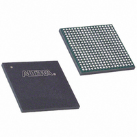
EP3C25F324I7 Altera, EP3C25F324I7 Datasheet - Page 125

EP3C25F324I7
Manufacturer Part Number
EP3C25F324I7
Description
IC CYCLONE III FPGA 25K 324 FBGA
Manufacturer
Altera
Series
Cyclone® IIIr
Datasheets
1.EP3C5F256C8N.pdf
(5 pages)
2.EP3C5F256C8N.pdf
(34 pages)
3.EP3C5F256C8N.pdf
(66 pages)
4.EP3C5F256C8N.pdf
(14 pages)
5.EP3C5F256C8N.pdf
(76 pages)
6.EP3C25F324I7.pdf
(274 pages)
Specifications of EP3C25F324I7
Number Of Logic Elements/cells
24624
Number Of Labs/clbs
1539
Total Ram Bits
608256
Number Of I /o
215
Voltage - Supply
1.15 V ~ 1.25 V
Mounting Type
Surface Mount
Operating Temperature
-40°C ~ 100°C
Package / Case
324-FBGA
Family Name
Cyclone III
Number Of Logic Blocks/elements
24624
# I/os (max)
215
Frequency (max)
437.5MHz
Process Technology
65nm
Operating Supply Voltage (typ)
1.2V
Logic Cells
24624
Ram Bits
608256
Operating Supply Voltage (min)
1.15V
Operating Supply Voltage (max)
1.25V
Operating Temp Range
-40C to 100C
Operating Temperature Classification
Industrial
Mounting
Surface Mount
Pin Count
324
Package Type
FBGA
For Use With
544-2370 - KIT STARTER CYCLONE III EP3C25
Lead Free Status / RoHS Status
Contains lead / RoHS non-compliant
Number Of Gates
-
Lead Free Status / Rohs Status
Not Compliant
Available stocks
Company
Part Number
Manufacturer
Quantity
Price
Company:
Part Number:
EP3C25F324I7N
Manufacturer:
ALTERA32
Quantity:
181
High-Speed I/O Interface
© December 2009
CIII51008-3.2
f
Altera Corporation
This chapter describes the high-speed differential I/O features and resources in the
Cyclone III device family.
High-speed differential I/O standards have become popular in high-speed interfaces
because of their significant advantages over single-ended I/O standards. The Altera
Cyclone
BLVDS, reduced swing differential signaling (RSDS), mini-LVDS, and point-to-point
differential signaling (PPDS).
This chapter contains the following sections:
■
■
■
■
■
■
Cyclone III device family I/Os are separated into eight I/O banks, as shown in
Figure
LVDS, RSDS, mini-LVDS, and PPDS are on the left and right I/O banks. These I/O
standards are also supported on the top and bottom I/O banks using external
resistors. On the left and right I/O banks, some of the differential pin pairs (p and n
pins) of the true output drivers are not located on adjacent pins. In these cases, a
power pin is located between the p and n pins. These I/O standards are also
supported on all I/O banks using two single-ended output with the second output
programmed as inverted, and an external resistor network. True input buffers for
these I/O standards are supported on all I/O banks.
For more information about the location of Cyclone III device family true differential
pins, refer to the
“High-Speed I/O Interface” on page 7–1
“High-Speed I/O Standards Support” on page 7–7
“True Output Buffer Feature” on page 7–15
“High-Speed I/O Timing” on page 7–16
“Design Guidelines” on page 7–17
“Software Overview” on page 7–18
7–1. Each bank has an independent power supply. True output drivers for
®
III device family (Cyclone III and Cyclone III LS devices) supports LVDS,
Cyclone III Devices Pin-Outs
7. High-Speed Differential Interfaces in
the Cyclone III Device Family
on the Altera website.
Cyclone III Device Handbook, Volume 1
®


