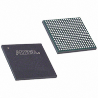
EP3C25F324I7 Altera, EP3C25F324I7 Datasheet - Page 215

EP3C25F324I7
Manufacturer Part Number
EP3C25F324I7
Description
IC CYCLONE III FPGA 25K 324 FBGA
Manufacturer
Altera
Series
Cyclone® IIIr
Datasheets
1.EP3C5F256C8N.pdf
(5 pages)
2.EP3C5F256C8N.pdf
(34 pages)
3.EP3C5F256C8N.pdf
(66 pages)
4.EP3C5F256C8N.pdf
(14 pages)
5.EP3C5F256C8N.pdf
(76 pages)
6.EP3C25F324I7.pdf
(274 pages)
Specifications of EP3C25F324I7
Number Of Logic Elements/cells
24624
Number Of Labs/clbs
1539
Total Ram Bits
608256
Number Of I /o
215
Voltage - Supply
1.15 V ~ 1.25 V
Mounting Type
Surface Mount
Operating Temperature
-40°C ~ 100°C
Package / Case
324-FBGA
Family Name
Cyclone III
Number Of Logic Blocks/elements
24624
# I/os (max)
215
Frequency (max)
437.5MHz
Process Technology
65nm
Operating Supply Voltage (typ)
1.2V
Logic Cells
24624
Ram Bits
608256
Operating Supply Voltage (min)
1.15V
Operating Supply Voltage (max)
1.25V
Operating Temp Range
-40C to 100C
Operating Temperature Classification
Industrial
Mounting
Surface Mount
Pin Count
324
Package Type
FBGA
For Use With
544-2370 - KIT STARTER CYCLONE III EP3C25
Lead Free Status / RoHS Status
Contains lead / RoHS non-compliant
Number Of Gates
-
Lead Free Status / Rohs Status
Not Compliant
Available stocks
Company
Part Number
Manufacturer
Quantity
Price
Company:
Part Number:
EP3C25F324I7N
Manufacturer:
ALTERA32
Quantity:
181
Chapter 9: Configuration, Design Security, and Remote System Upgrades in the Cyclone III Device Family
Configuration Features
Figure 9–27. JTAG Configuration of Multiple Devices Using a Download Cable (1.2, 1.5, and 1.8-V V
Pins)
Notes to
(1) Connect these pull-up resistors to the V
(2) Connect the nCONFIG and MSEL[3..0] pins to support a non-JTAG configuration scheme. If you only use a JTAG configuration, connect the
(3) In the USB-Blaster and ByteBlaster II cable, this pin is connected to nCE when it is used for AS programming, otherwise it is a no connect.
(4) The nCE pin must be connected to ground or driven low for successful JTAG configuration.
(5) Power up the V
© December 2009
Pin 1
10-Pin Male Header
Download Cable
nCONFIG pin to logic high and the MSEL[3..0] pins to ground. In addition, pull DCLK and DATA[0] either high or low, whichever is
convenient on your board.
target supply voltage of 1.2 V. For the target supply voltage value, refer to the
Download Cable User
V
Figure
CCIO
(5)
10 kΩ
VIO
V
(3)
9–27:
CCIO (1)
1 kΩ
1
CC
Altera Corporation
V
of the ByteBlaster II or USB-Blaster cable with supply from V
CCIO (1)
10 kΩ
Guide.
All I/O inputs must maintain a maximum AC voltage of 4.1 V. If a non-Cyclone III
device family is cascaded in the JTAG-chain, TDO of the non-Cyclone III device family
driving into TDI of the Cyclone III device family must fit the maximum overshoot
equation outlined in
The nCE pin must be connected to GND or driven low during JTAG configuration. In
multi-device AS, AP, PS, and FPP configuration chains, the nCE pin of the first device
is connected to GND while its nCEO pin is connected to the nCE pin of the next device
in the chain. The inputs of the nCE pin of the last device come from the previous
device while its nCEO pin is left floating. In addition, the CONF_DONE and nSTATUS
signals are shared in multi-device AS, AP, PS, and FPP configuration chains to ensure
that the devices enter user mode at the same time after configuration is complete.
When the CONF_DONE and nSTATUS signals are shared among all the devices, every
device must be configured when you perform JTAG configuration.
If you only use JTAG configuration, Altera recommends that you connect the circuitry
as shown in
nSTATUS signals are isolated so that each device can enter user mode individually.
(2)
(2)
(2)
(2)
(2)
V
CCIO
10
(1)
nST A TUS
DATA[0]
DCLK
nCONFIG
MSEL[3..0]
nCEO
nCE
TDI
kΩ
TMS
(4)
Device Family
CCIO
Cyclone III
Figure 9–26
TCK
CONF_DONE
supply of the bank in which the pin resides.
TDO
“Configuration and JTAG Pin I/O Requirements” on page
V
CCIO
or
10
(1)
Figure
kΩ
(2)
(2)
(2)
(2)
(2)
V
CCIO
9–27, in which each of the CONF_DONE and
10
(1)
DATA[0]
DCLK
MSEL[3..0]
nCE
TDI
nST A TUS
nCONFIG
nCEO
kΩ
TMS
ByteBlaster II Download Cable User Guide
(4)
CCIO
Device Family
. The ByteBlaster II and USB-Blaster cables do not support a
Cyclone III
TCK
CONF_DONE
TDO
V
CCIO
10
(1)
kΩ
Cyclone III Device Handbook, Volume 1
(2)
(2)
(2)
(2)
(2)
V
CCIO
10
CCIO
(1)
nST A TUS
DATA[0]
DCLK
nCONFIG
MSEL[3..0]
nCEO
nCE
TDI
kΩ
TMS
Powering the JTAG
(4)
and the
Device Family
Cyclone III
CONF_DONE
TCK
USB-Blaster
TDO
9–7.
V
CCIO
9–55
10
(1)
kΩ


