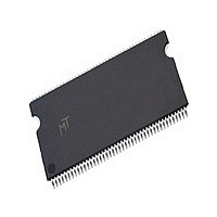
MT48LC8M32B2P-6 Micron Technology Inc, MT48LC8M32B2P-6 Datasheet - Page 31

MT48LC8M32B2P-6
Manufacturer Part Number
MT48LC8M32B2P-6
Description
Manufacturer
Micron Technology Inc
Type
SDRAMr
Datasheet
1.MT48LC8M32B2P-6.pdf
(56 pages)
Specifications of MT48LC8M32B2P-6
Organization
8Mx32
Density
256Mb
Address Bus
14b
Access Time (max)
17/7.5/5.5ns
Maximum Clock Rate
166MHz
Operating Supply Voltage (typ)
3.3V
Package Type
TSOP
Operating Temp Range
0C to 70C
Operating Supply Voltage (max)
3.6V
Operating Supply Voltage (min)
3V
Supply Current
165mA
Pin Count
86
Mounting
Surface Mount
Operating Temperature Classification
Commercial
Lead Free Status / Rohs Status
Compliant
Available stocks
Company
Part Number
Manufacturer
Quantity
Price
Company:
Part Number:
MT48LC8M32B2P-6
Manufacturer:
MIC
Quantity:
1 000
Company:
Part Number:
MT48LC8M32B2P-6
Manufacturer:
MIC
Quantity:
1 000
Company:
Part Number:
MT48LC8M32B2P-6F
Manufacturer:
MIC
Quantity:
1 000
Company:
Part Number:
MT48LC8M32B2P-6F
Manufacturer:
MIC
Quantity:
1 000
Company:
Part Number:
MT48LC8M32B2P-6G
Manufacturer:
MIC
Quantity:
1 000
Table 9:
Notes 1–17; notes appear below and on next page
NOTE:
09005aef8140ad6d
MT48LC8M32B2_2.fm - Rev. B 10/04 EN
CURRENT STATE
Any
Idle
Row Activating,
Active, or Precharging
Read
(Auto Precharge
Disabled)
Write
(Auto Precharge
Disabled)
Read
(With Auto Precharge)
Write
(With Auto Precharge)
1. This table applies when CKE
2. This table describes alternate bank operation, except where noted; i.e., the current state is for bank n and the com-
3. Current state definitions:
4. AUTO REFRESH, SELF REFRESH, and LOAD MODE REGISTER commands may only be issued when all banks are idle.
5. A BURST TERMINATE command cannot be issued to another bank; it applies to the bank represented by the current
6. All states and sequences not shown are illegal or reserved.
state was self refresh).
mands shown are those allowed to be issued to bank m (assuming that bank m is in such a state that the given com-
mand is allowable). Exceptions are covered in the notes below.
state only.
Idle:
Row Active:
Read:
Write:
Read with
auto precharge
enabled:
Truth Table 4 – Current State Bank n, Command To Bank m
CS# RAS# CAS# WE#
H
X
L
L
L
L
L
L
L
L
L
L
L
L
L
L
L
L
L
L
L
L
L
The bank has been precharged, and
A row in the bank has been activated, and
accesses and no regster accesses are in progress.
A READ burst has been initiated, with auto precharge disabled, and has not yet ter
minated or been terminated.
A WRITE burst has been initiated, with auto precharge disabled, and has not yet
terminated or been terminated.
Starts with registration of a READ command with auto precharge enabled, and
ends when
n-1
H
H
H
H
H
H
H
H
H
H
H
X
X
L
L
L
L
L
L
L
L
L
L
was HIGH and CKE
H
H
H
H
H
H
H
H
H
H
H
X
X
L
L
L
L
L
L
L
L
L
L
t
RP has been met. Once
H
H
H
H
H
H
H
H
H
H
H
X
X
L
L
L
L
L
L
L
L
L
L
n
COMMAND INHIBIT (NOP/Continue previous operation)
NO OPERATION (NOP/Continue previous operation)
Any Command Otherwise Allowed to Bank m
ACTIVE (Select and activate row)
READ (Select column and start READ burst)
WRITE (Select column and start WRITE burst)
PRECHARGE
ACTIVE (Select and activate row)
READ (Select column and start new READ burst)
WRITE (Select column and start WRITE burst)
PRECHARGE
ACTIVE (Select and activate row)
READ (Select column and start READ burst)
WRITE (Select column and start new WRITE burst)
PRECHARGE
ACTIVE (Select and activate row)
READ (Select column and start new READ burst)
WRITE (Select column and start WRITE burst)
PRECHARGE
ACTIVE (Select and activate row)
READ (Select column and start READ burst)
WRITE (Select column and start new WRITE burst)
PRECHARGE
is HIGH (see Table 7) and after
31
t
RP is met, the bank will be in the idle state.
t
RP has been met.
Micron Technology, Inc., reserves the right to change products or specifications without notice.
COMMAND (ACTION)
t
RCD has been met. No data bursts/
t
XSR has been met (if the previous
©2003 Micron Technology, Inc. All rights reserved.
256Mb: x32
SDRAM
NOTES
7, 8, 14
7, 8, 15
7, 8, 16
7, 8, 17
7, 10
7, 11
7, 12
7, 13
7
7
9
9
9
9


