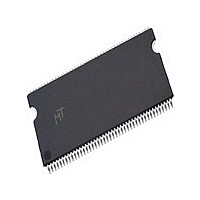
MT48LC8M32B2P-6 Micron Technology Inc, MT48LC8M32B2P-6 Datasheet - Page 19

MT48LC8M32B2P-6
Manufacturer Part Number
MT48LC8M32B2P-6
Description
Manufacturer
Micron Technology Inc
Type
SDRAMr
Datasheet
1.MT48LC8M32B2P-6.pdf
(56 pages)
Specifications of MT48LC8M32B2P-6
Organization
8Mx32
Density
256Mb
Address Bus
14b
Access Time (max)
17/7.5/5.5ns
Maximum Clock Rate
166MHz
Operating Supply Voltage (typ)
3.3V
Package Type
TSOP
Operating Temp Range
0C to 70C
Operating Supply Voltage (max)
3.6V
Operating Supply Voltage (min)
3V
Supply Current
165mA
Pin Count
86
Mounting
Surface Mount
Operating Temperature Classification
Commercial
Lead Free Status / Rohs Status
Compliant
Available stocks
Company
Part Number
Manufacturer
Quantity
Price
Company:
Part Number:
MT48LC8M32B2P-6
Manufacturer:
MIC
Quantity:
1 000
Company:
Part Number:
MT48LC8M32B2P-6
Manufacturer:
MIC
Quantity:
1 000
Company:
Part Number:
MT48LC8M32B2P-6F
Manufacturer:
MIC
Quantity:
1 000
Company:
Part Number:
MT48LC8M32B2P-6F
Manufacturer:
MIC
Quantity:
1 000
Company:
Part Number:
MT48LC8M32B2P-6G
Manufacturer:
MIC
Quantity:
1 000
NOTE:
The DQM input is used to avoid I/O contention, as
shown in Figures 12 and 13. DQM must be asserted
(HIGH) at least two clocks prior to the WRITE com-
mand (DQM latency is two clocks for output buffers)
to suppress data-out from the READ. Once the WRITE
command is registered, the DQs will go High-Z (or
remain High-Z), regardless of the state of the DQMs.
The DQs remain High-Z, provided DQM was active on
the clock just prior to the WRITE command that trun-
cated the READ command. If not, the second WRITE
will be an invalid WRITE. For example, if DQM was
LOW during T4 (in Figure 13), then the WRITEs at T5
and T7 would be valid, while the WRITE at T6 would be
invalid.
The DQM signal must be de-asserted prior to the
WRITE command (DQM latency is zero clocks for
input buffers) to ensure that the written data is not
masked. Figure 12 shows the case where the clock fre-
quency allows for bus contention to be avoided with-
out adding a NOP cycle, and Figure 13 shows the case
where the additional NOP is needed.
09005aef8140ad6d
MT48LC8M32B2_2.fm - Rev. B 10/04 EN
CL = 3 is used for illustration. The READ command may
be to any bank, and the WRITE command may be to any
bank. If a burst of one is used, then DQM is not
required.
COMMAND
ADDRESS
DQM
Figure 12: READ-to-WRITE
CLK
DQ
T0
BANK,
COL n
READ
T1
NOP
T2
NOP
T3
NOP
D
t HZ
OUT
t CK
n
DON’T CARE
T4
BANK,
COL b
WRITE
D
IN
b
t
DS
19
NOTE:
A fixed-length READ burst may be followed by, or trun-
cated with, a PRECHARGE command to the same bank
(provided that auto precharge was not activated), and
a full-page burst may be truncated with a PRECHARGE
command to the same bank. The PRECHARGE com-
mand should be issued x cycles before the clock edge
at which the last desired data element is valid, where x
equals the CAS latency minus one. This is shown in
Figure 14 on page 20 for each possible CAS latency;
data element n + 3 is either the last of a burst of four or
the last desired of a longer burst. Following the PRE-
CHARGE command, a subsequent command to the
same bank cannot be issued until
part of the row precharge time is hidden during the
access of the last data element(s).
In the case of a fixed-length burst being executed to
completion, a PRECHARGE command issued at the
optimum time (as described above) provides the same
operation that would result from the same fixed-length
burst with auto precharge. The disadvantage of the
PRECHARGE command is that it requires that the
command and address buses be available at the
appropriate time to issue the command; the advantage
of the PRECHARGE command is that it can be used to
truncate fixed-length or full-page bursts.
COMMAND
Figure 13: READ-to-WRITE with Extra
CL = 3 is used for illustration. The READ command may
be to any bank, and the WRITE command may be to any
bank.
ADDRESS
DQM
Micron Technology, Inc., reserves the right to change products or specifications without notice.
CLK
DQ
BANK,
COL n
T0
READ
T1
Clock Cycle
NOP
T2
NOP
©2003 Micron Technology, Inc. All rights reserved.
T3
256Mb: x32
NOP
t
RP is met. Note that
t HZ
D
OUT
n
T4
SDRAM
NOP
DON’T CARE
T5
BANK,
COL b
WRITE
D
IN
b
t
DS


