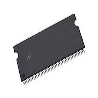
MT48LC8M32B2P-6 Micron Technology Inc, MT48LC8M32B2P-6 Datasheet - Page 26

MT48LC8M32B2P-6
Manufacturer Part Number
MT48LC8M32B2P-6
Description
Manufacturer
Micron Technology Inc
Type
SDRAMr
Datasheet
1.MT48LC8M32B2P-6.pdf
(56 pages)
Specifications of MT48LC8M32B2P-6
Organization
8Mx32
Density
256Mb
Address Bus
14b
Access Time (max)
17/7.5/5.5ns
Maximum Clock Rate
166MHz
Operating Supply Voltage (typ)
3.3V
Package Type
TSOP
Operating Temp Range
0C to 70C
Operating Supply Voltage (max)
3.6V
Operating Supply Voltage (min)
3V
Supply Current
165mA
Pin Count
86
Mounting
Surface Mount
Operating Temperature Classification
Commercial
Lead Free Status / Rohs Status
Compliant
Available stocks
Company
Part Number
Manufacturer
Quantity
Price
Company:
Part Number:
MT48LC8M32B2P-6
Manufacturer:
MIC
Quantity:
1 000
Company:
Part Number:
MT48LC8M32B2P-6
Manufacturer:
MIC
Quantity:
1 000
Company:
Part Number:
MT48LC8M32B2P-6F
Manufacturer:
MIC
Quantity:
1 000
Company:
Part Number:
MT48LC8M32B2P-6F
Manufacturer:
MIC
Quantity:
1 000
Company:
Part Number:
MT48LC8M32B2P-6G
Manufacturer:
MIC
Quantity:
1 000
NOTE:
NOTE:
WRITE with AUTO PRECHARGE
3. Interrupted by a READ (with or without auto pre-
charge): A READ to bank m will interrupt a WRITE on
bank n when registered, with the data-out appearing
CAS latency later. The PRECHARGE to bank n will
begin after
READ to bank m is registered. The last valid WRITE to
bank n will be data-in registered one clock prior to the
READ to bank m (Figure 29).
09005aef8140ad6d
MT48LC8M32B2_2.fm - Rev. B 10/04 EN
DQM is LOW.
DQM is HIGH at T2 to prevent D
t
WR is met, where
Figure 28: READ With Auto Precharge Interrupted by a WRITE
Figure 27: READ With Auto Precharge Interrupted by a READ
Internal
States
Internal
States
COMMAND
COMMAND
ADDRESS
BANK m
ADDRESS
BANK n
BANK m
t
BANK n
DQM
OUT
WR begins when the
CLK
DQ
CLK
DQ
1
- a + 1 from contending with D
Active
Page
READ - AP
BANK n,
BANK n
COL a
T0
Page Active
T0
NOP
READ with Burst of 4
CL = 3 (BANK n )
Page Active
READ - AP
T1
NOP
BANK n,
Page Active
BANK n
COL a
T1
READ with Burst of 4
CL = 3 (BANK n)
T2
NOP
T2
NOP
26
4. Interrupted by a WRITE (with or without auto pre-
charge): A WRITE to bank m will interrupt a WRITE on
bank n when registered. The PRECHARGE to bank n
will begin after
WRITE to bank m is registered. The last valid data
WRITE to bank n will be data registered one clock prior
to a WRITE to bank m (Figure 30).
T3
BANK m,
D
READ - AP
NOP
T3
BANK m
COL d
OUT
a
Interrupt Burst, Precharge
CL = 3 (BANK m)
READ with Burst of 4
Micron Technology, Inc., reserves the right to change products or specifications without notice.
IN
BANK m,
WRITE - AP
COL d
BANK m
T4
- d at T4.
D
d
T4
IN
Interrupt Burst, Precharge
NOP
WRITE with Burst of 4
D
OUT
a
t
RP - BANK n
T5
d + 1
NOP
T5
D
t
IN
NOP
WR is met, where
D
a + 1
t
RP - BANK n
OUT
T6
d + 2
NOP
D
T6
IN
NOP
D
OUT
d
DON’T CARE
DON’T CARE
Idle
T7
t WR - BANK m
d + 3
NOP
©2003 Micron Technology, Inc. All rights reserved.
D
T7
IN
NOP
Write-Back
t RP - BANK m
Precharge
D
d + 1
Idle
OUT
256Mb: x32
t
WR begins when the
SDRAM


