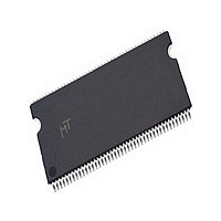
MT48LC8M32B2P-6 Micron Technology Inc, MT48LC8M32B2P-6 Datasheet - Page 14

MT48LC8M32B2P-6
Manufacturer Part Number
MT48LC8M32B2P-6
Description
Manufacturer
Micron Technology Inc
Type
SDRAMr
Datasheet
1.MT48LC8M32B2P-6.pdf
(56 pages)
Specifications of MT48LC8M32B2P-6
Organization
8Mx32
Density
256Mb
Address Bus
14b
Access Time (max)
17/7.5/5.5ns
Maximum Clock Rate
166MHz
Operating Supply Voltage (typ)
3.3V
Package Type
TSOP
Operating Temp Range
0C to 70C
Operating Supply Voltage (max)
3.6V
Operating Supply Voltage (min)
3V
Supply Current
165mA
Pin Count
86
Mounting
Surface Mount
Operating Temperature Classification
Commercial
Lead Free Status / Rohs Status
Compliant
Available stocks
Company
Part Number
Manufacturer
Quantity
Price
Company:
Part Number:
MT48LC8M32B2P-6
Manufacturer:
MIC
Quantity:
1 000
Company:
Part Number:
MT48LC8M32B2P-6
Manufacturer:
MIC
Quantity:
1 000
Company:
Part Number:
MT48LC8M32B2P-6F
Manufacturer:
MIC
Quantity:
1 000
Company:
Part Number:
MT48LC8M32B2P-6F
Manufacturer:
MIC
Quantity:
1 000
Company:
Part Number:
MT48LC8M32B2P-6G
Manufacturer:
MIC
Quantity:
1 000
READ
The READ command is used to initiate a burst read
access to an active row. The value on the BA0 and BA1
(B1) inputs selects the bank, and the address provided
on inputs A0–A8 selects the starting column location.
The value on input A10 determines whether or not
auto precharge is used. If auto precharge is selected,
the row being accessed will be precharged at the end of
the READ burst; if auto precharge is not selected, the
row will remain open for subsequent accesses. Read
data appears on the DQs subject to the logic level on
the DQM inputs two clocks earlier. If a given DQMx
signal was registered HIGH, the corresponding DQs
will be High-Z two clocks later; if the DQMx signal was
registered LOW, the corresponding DQs will provide
valid data. DQM0 corresponds to DQ0–DQ7, DQM1
corresponds to DQ8–DQ15, DQM2 corresponds to
DQ16–DQ23, and DQM3 corresponds to DQ24–DQ31.
WRITE
The WRITE command is used to initiate a burst write
access to an active row. The value on the BA0 and BA1
inputs selects the bank, and the address provided on
inputs A0–A8 selects the starting column location. The
value on input A10 determines whether or not auto
precharge is used. If auto precharge is selected, the row
being accessed will be precharged at the end of the
WRITE burst; if auto precharge is not selected, the row
will remain open for subsequent accesses. Input data
appearing on the DQs is written to the memory array
subject to the DQM input logic level appearing coinci-
dent with the data. If a given DQM signal is registered
LOW, the corresponding data will be written to mem-
ory; if the DQM signal is registered HIGH, the corre-
sponding data inputs will be ignored, and a WRITE will
not be executed to that byte/column location.
PRECHARGE
The PRECHARGE command is used to deactivate the
open row in a particular bank or the open row in all
banks. The bank(s) will be available for a subsequent
row access a specified time (
command is issued. Input A10 determines whether
one or all banks are to be precharged, and in the case
where only one bank is to be precharged, inputs BA0
and BA1 select the bank. Otherwise BA0 and BA1 are
treated as “Don’t Care.” Once a bank has been pre-
charged, it is in the idle state and must be activated
prior to any READ or WRITE commands being issued
to that bank.
09005aef8140ad6d
MT48LC8M32B2_2.fm - Rev. B 10/04 EN
t
RP) after the PRECHARGE
14
AUTO PRECHARGE
Auto precharge is a feature which performs the same
individual bank PRECHARGE function described
above, without requiring an explicit command. This is
accomplished by using A10 to enable auto precharge
in conjunction with a specific READ or WRITE com-
mand. A PRECHARGE of the bank/row that is
addressed with the READ or WRITE command is auto-
matically performed upon completion of the READ or
WRITE burst, except in the full-page burst mode,
where auto precharge does not apply. Auto precharge
is nonpersistent in that it is either enabled or disabled
for each individual READ or WRITE command.
Auto precharge ensures that the precharge is initiated
at the earliest valid stage within a burst. The user must
not issue another command to the same bank until the
precharge time (
as if an explicit PRECHARGE command was issued at
the earliest possible time, as described for each burst
type in “Operations” on page 15.
BURST TERMINATE
The BURST TERMINATE command is used to truncate
either fixed-length or full-page bursts. The most
recently registered READ or WRITE command prior to
the BURST TERMINATE command will be truncated,
as shown in “Operations” on page 15.
AUTO REFRESH
AUTO REFRESH is used during normal operation of
the SDRAM and is analogous to CAS#-BEFORE-RAS#
(CBR) REFRESH in conventional DRAMs. This com-
mand is nonpersistent, so it must be issued each time
a refresh is required.
The addressing is generated by the internal refresh
controller. This makes the address bits “Don’t Care”
during an AUTO REFRESH command. The 256Mb
SDRAM requires 4,096 AUTO REFRESH cycles every
64ms (
distributed AUTO REFRESH command every 15.625µs
will meet the refresh requirement and ensure that each
row is refreshed. Alternatively, 4,096 AUTO REFRESH
commands can be issued in a burst at the minimum
cycle rate (
SELF REFRESH
The SELF REFRESH command can be used to retain
data in the SDRAM, even if the rest of the system is
powered down. When in the self refresh mode, the
SDRAM retains data without external clocking. The
SELF REFRESH command is initiated like an AUTO
REFRESH command except CKE is disabled (LOW).
Micron Technology, Inc., reserves the right to change products or specifications without notice.
t
REF), regardless of width option. Providing a
t
RFC), once every 64ms.
t
RP) is completed. This is determined
©2003 Micron Technology, Inc. All rights reserved.
256Mb: x32
SDRAM


