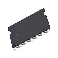
MT48LC8M32B2P-6 Micron Technology Inc, MT48LC8M32B2P-6 Datasheet - Page 10

MT48LC8M32B2P-6
Manufacturer Part Number
MT48LC8M32B2P-6
Description
Manufacturer
Micron Technology Inc
Type
SDRAMr
Datasheet
1.MT48LC8M32B2P-6.pdf
(56 pages)
Specifications of MT48LC8M32B2P-6
Organization
8Mx32
Density
256Mb
Address Bus
14b
Access Time (max)
17/7.5/5.5ns
Maximum Clock Rate
166MHz
Operating Supply Voltage (typ)
3.3V
Package Type
TSOP
Operating Temp Range
0C to 70C
Operating Supply Voltage (max)
3.6V
Operating Supply Voltage (min)
3V
Supply Current
165mA
Pin Count
86
Mounting
Surface Mount
Operating Temperature Classification
Commercial
Lead Free Status / Rohs Status
Compliant
Available stocks
Company
Part Number
Manufacturer
Quantity
Price
Company:
Part Number:
MT48LC8M32B2P-6
Manufacturer:
MIC
Quantity:
1 000
Company:
Part Number:
MT48LC8M32B2P-6
Manufacturer:
MIC
Quantity:
1 000
Company:
Part Number:
MT48LC8M32B2P-6F
Manufacturer:
MIC
Quantity:
1 000
Company:
Part Number:
MT48LC8M32B2P-6F
Manufacturer:
MIC
Quantity:
1 000
Company:
Part Number:
MT48LC8M32B2P-6G
Manufacturer:
MIC
Quantity:
1 000
Functional Description
In general, this 256Mb SDRAM (2 Meg x 32 x 4 banks) is
a quad-bank DRAM that operates at 3.3V and includes
a synchronous interface (all signals are registered on
the positive edge of the clock signal, CLK). Each of the
67,108,864-bit banks is organized as 4,096 rows by 512
columns by 32-bits.
Read and write accesses to the SDRAM are burst ori-
ented; accesses start at a selected location and con-
tinue for a programmed number of locations in a
programmed sequence. Accesses begin with the regis-
tration of an ACTIVE command, which is then fol-
lowed by a READ or WRITE command. The address
bits registered coincident with the ACTIVE command
are used to select the bank and row to be accessed
(BA0 and BA1 select the bank, A0–A11 select the row).
The address bits (A0–A8) registered coincident with
the READ or WRITE command are used to select the
starting column location for the burst access.
Prior to normal operation, the SDRAM must be initial-
ized. The following sections provide detailed informa-
tion covering device initialization, register definition,
command descriptions, and device operation.
Initialization
SDRAMs must be powered up and initialized in a pre-
defined manner. Operational procedures other than
those specified may result in undefined operation.
Once power is applied to V
neously) and the clock is stable (stable clock is defined
as a signal cycling within timing constraints specified
for the clock pin), the SDRAM requires a 100µs delay
prior to issuing any command other than a COM-
MAND INHIBIT or a NOP . Starting at some point dur-
ing this 100µs period and continuing at least through
the end of this period, COMMAND INHIBIT or NOP
commands should be applied.
Once the 100µs delay has been satisfied with at least
one COMMAND INHIBIT or NOP command having
been applied, a PRECHARGE command should be
applied. All banks must then be precharged, thereby
placing the device in the all banks idle state.
Once in the idle state, two AUTO REFRESH cycles must
be performed. After the AUTO REFRESH cycles are
complete, the SDRAM is ready for mode register pro-
gramming. Because the mode register will power up in
an unknown state, it should be loaded prior to apply-
ing any operational command.
09005aef8140ad6d
MT48LC8M32B2_2.fm - Rev. B 10/04 EN
DD
and V
DD
Q (simulta-
10
Register Definition
Mode Register
The mode register is used to define the specific mode
of operation of the SDRAM. This definition includes
the selection of a burst length, a burst type, a CAS
latency, an operating mode, and a write burst mode, as
shown in Figure 1. The mode register is programmed
via the LOAD MODE REGISTER command and will
retain the stored information until it is programmed
again or the device loses power.
Mode register bits M0–M2 specify the burst length, M3
specifies the type of burst (sequential or interleaved),
M4–M6 specify the CAS latency, M7 and M8 specify the
operating mode, M9 specifies the write burst mode,
and M10, M11, BA0, and BA1 are reserved for future
use.
The mode register must be loaded when all banks are
idle, and the controller must wait the specified time
before initiating the subsequent operation. Violating
either of these requirements will result in unspecified
operation.
Burst Length
Read and write accesses to the SDRAM are burst ori-
ented, with the burst length being programmable, as
shown in Figure 1. The burst length determines the
maximum number of column locations that can be
accessed for a given READ or WRITE command. Burst
lengths of 1, 2, 4, or 8 locations are available for both
the sequential and the interleaved burst types, and a
full-page burst is available for the sequential type. The
full-page burst is used in conjunction with the BURST
TERMINATE command to generate arbitrary burst
lengths.
Reserved states should not be used, as unknown oper-
ation or incompatibility with future versions may
result.
When a READ or WRITE command is issued, a block of
columns equal to the burst length is effectively
selected. All accesses for that burst take place within
this block, meaning that the burst will wrap within the
block if a boundary is reached. The block is uniquely
selected by A1–A8 when the burst length is set to two;
by A2–A8 when the burst length is set to four; and by
A3–A8 when the burst length is set to eight. The
remaining (least significant) address bit(s) is (are) used
to select the starting location within the block. Full-
page bursts wrap within the page if the boundary is
reached.
Micron Technology, Inc., reserves the right to change products or specifications without notice.
©2003 Micron Technology, Inc. All rights reserved.
256Mb: x32
SDRAM


