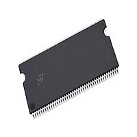
MT48LC8M32B2P-6 Micron Technology Inc, MT48LC8M32B2P-6 Datasheet - Page 21

MT48LC8M32B2P-6
Manufacturer Part Number
MT48LC8M32B2P-6
Description
Manufacturer
Micron Technology Inc
Type
SDRAMr
Datasheet
1.MT48LC8M32B2P-6.pdf
(56 pages)
Specifications of MT48LC8M32B2P-6
Organization
8Mx32
Density
256Mb
Address Bus
14b
Access Time (max)
17/7.5/5.5ns
Maximum Clock Rate
166MHz
Operating Supply Voltage (typ)
3.3V
Package Type
TSOP
Operating Temp Range
0C to 70C
Operating Supply Voltage (max)
3.6V
Operating Supply Voltage (min)
3V
Supply Current
165mA
Pin Count
86
Mounting
Surface Mount
Operating Temperature Classification
Commercial
Lead Free Status / Rohs Status
Compliant
Available stocks
Company
Part Number
Manufacturer
Quantity
Price
Company:
Part Number:
MT48LC8M32B2P-6
Manufacturer:
MIC
Quantity:
1 000
Company:
Part Number:
MT48LC8M32B2P-6
Manufacturer:
MIC
Quantity:
1 000
Company:
Part Number:
MT48LC8M32B2P-6F
Manufacturer:
MIC
Quantity:
1 000
Company:
Part Number:
MT48LC8M32B2P-6F
Manufacturer:
MIC
Quantity:
1 000
Company:
Part Number:
MT48LC8M32B2P-6G
Manufacturer:
MIC
Quantity:
1 000
NOTE:
WRITEs
WRITE bursts are initiated with a WRITE command, as
shown in Figure 16 on page 22.
The starting column and bank addresses are provided
with the WRITE command, and auto precharge is
either enabled or disabled for that access. If auto pre-
charge is enabled, the row being accessed is pre-
charged at the completion of the burst. For the generic
WRITE commands used in the following illustrations,
auto precharge is disabled.
09005aef8140ad6d
MT48LC8M32B2_2.fm - Rev. B 10/04 EN
DQM is LOW.
COMMAND
COMMAND
COMMAND
ADDRESS
ADDRESS
ADDRESS
CLK
CLK
CLK
DQ
DQ
DQ
Figure 15: Terminating a READ Burst
BANK,
BANK,
COL n
COL n
T0
T0
T0
BANK,
COL n
READ
READ
READ
CL = 1
CL = 2
T1
T1
T1
NOP
NOP
NOP
D
OUT
n
CL = 3
T2
T2
T2
NOP
NOP
NOP
D
D
n + 1
OUT
OUT
n
T3
T3
T3
21
NOP
NOP
NOP
D
n + 2
D
D
n + 1
OUT
OUT
OUT
n
During WRITE bursts, the first valid data-in element
will be registered coincident with the WRITE com-
mand. Subsequent data elements will be registered on
each successive positive clock edge. Upon completion
of a fixed-length burst, assuming no other commands
have been initiated, the DQs will remain High-Z and
any additional input data will be ignored (see Figure 17
on page 22). A full-page burst will continue until termi-
nated. (At the end of the page, it will wrap to column 0
and continue.) Data for any WRITE burst may be trun-
cated with a subsequent WRITE command, and data
TERMINATE
TERMINATE
TERMINATE
T4
BURST
T4
BURST
T4
BURST
X = 0 cycles
X = 1 cycle
D
n + 2
D
n + 3
D
n + 1
OUT
Micron Technology, Inc., reserves the right to change products or specifications without notice.
OUT
OUT
X = 2 cycles
T5
T5
T5
NOP
NOP
NOP
D
n + 3
D
n + 2
OUT
OUT
T6
T6
T6
NOP
NOP
NOP
D
n + 3
OUT
DON’T CARE
T7
NOP
©2003 Micron Technology, Inc. All rights reserved.
256Mb: x32
SDRAM


