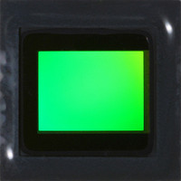
MT9P401I12STC Aptina LLC, MT9P401I12STC Datasheet - Page 8

MT9P401I12STC
Manufacturer Part Number
MT9P401I12STC
Description
SENSOR IMAGE CMOS 5MP 48LCC
Manufacturer
Aptina LLC
Type
CMOS Imagingr
Series
DigitalClarity®r
Specifications of MT9P401I12STC
Pixel Size
2.2µm x 2.2µm
Active Pixel Array
2592H x 1944V
Frames Per Second
60
Voltage - Supply
2.6 V ~ 3.1 V
Package / Case
48-iLCC
Sensor Image Color Type
Monochrome
Sensor Image Size
2592x1944Pixels
Operating Supply Voltage (typ)
1.8/2.8V
Operating Supply Voltage (max)
3.1V
Operating Temp Range
-30C to 70C
Package Type
ILCC
Operating Temperature Classification
Commercial
Mounting
Surface Mount
Pin Count
48
Lead Free Status / RoHS Status
Lead free / RoHS Compliant
Other names
557-1263
MT9P401I12STC
Q3412742
MT9P401I12STC
Q3412742
Available stocks
Company
Part Number
Manufacturer
Quantity
Price
Part Number:
MT9P401I12STC
Manufacturer:
APTINA
Quantity:
20 000
Table 3:
PDF: 09005aef82acb06f/Source: 09005aef81a4a477
MT9P401_DS_2 - Rev. B 9/07 EN
STANDBY_BAR
FRAME_VALID
LINE_VALID
RESET_BAR
D
TRIGGER
VAA_PIX
V
STROBE
EXTCLK
OUT
V
PIXCLK
Name
S
S
DD
D
A
RSVD
SCLK
TEST
DD
V
V
ADDR
DATA
OE
NC
GND
GND
DD
AA
[11:0]
_PLL
_IO
Pin Description
Output
Output
Output
Output
Output
Supply
Supply
Supply
Supply
Supply
Supply
Supply
Input
Input
Input
Input
Input
Input
Input
Type
I/O
—
—
—
Description
When LOW, the MT9P401 asynchronously resets. When driven HIGH, it resumes
normal operation with all configuration registers set to factory defaults.
External input clock.
Serial clock. Pull to V
When HIGH, the PIXCLK, D
driven LOW, normal operation resumes.
Standby. When LOW, the chip enters a low-power standby mode. It resumes
normal operation when the pin is driven HIGH.
Snapshot trigger. Used to trigger one frame of output in snapshot modes, and to
indicate the end of exposure in bulb exposure modes.
Serial address. When HIGH, the MT9P401 responds to device ID (BA)
it responds to serial device ID (90)
Serial data. Pull to V
Pixel clock. The D
falling edge of this signal.
Pixel data. Pixel data is 12-bit. MSB (D
be captured on the falling edge of PIXCLK.
Frame valid. Driven HIGH during active pixels and horizontal blanking of each
frame and LOW during vertical blanking.
Line valid. Driven HIGH with active pixels of each line and LOW during blanking
periods.
Snapshot strobe. Driven HIGH when all pixels are exposing in snapshot modes.
Digital supply voltage. Nominally 1.8V.
IO supply voltage. Nominally 1.8 or 2.8V.
Digital ground.
Analog supply voltage. Nominally 2.8V.
Pixel supply voltage. Nominally 2.8V, connected externally to V
Analog ground.
PLL supply voltage. Nominally 2.8V, connected externally to V
Tie to A
Tie to D
No connect.
Micron Confidential and Proprietary
GND
GND
for normal device operation (factory use only).
for normal device operation (factory use only).
MT9P401: 1/2.5-Inch 5Mp Digital Image Sensor
OUT
8
DD
DD
, FV, LV, and STROBE outputs should be captured on the
_IO with a 1.5
_IO with a 1.5
OUT
Micron Technology, Inc., reserves the right to change products or specifications without notice.
, FV, LV, and STROBE outputs enter a High-Z. When
H
.
kΩ
kΩ
OUT
resistor.
resistor.
11) through LSB (D
Functional Overview
©2007 Micron Technology, Inc. All rights reserved.
OUT
AA
AA
0) of each pixel, to
.
.
H
. When LOW,


