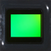
MT9P401I12STC Aptina LLC, MT9P401I12STC Datasheet - Page 26

MT9P401I12STC
Manufacturer Part Number
MT9P401I12STC
Description
SENSOR IMAGE CMOS 5MP 48LCC
Manufacturer
Aptina LLC
Type
CMOS Imagingr
Series
DigitalClarity®r
Specifications of MT9P401I12STC
Pixel Size
2.2µm x 2.2µm
Active Pixel Array
2592H x 1944V
Frames Per Second
60
Voltage - Supply
2.6 V ~ 3.1 V
Package / Case
48-iLCC
Sensor Image Color Type
Monochrome
Sensor Image Size
2592x1944Pixels
Operating Supply Voltage (typ)
1.8/2.8V
Operating Supply Voltage (max)
3.1V
Operating Temp Range
-30C to 70C
Package Type
ILCC
Operating Temperature Classification
Commercial
Mounting
Surface Mount
Pin Count
48
Lead Free Status / RoHS Status
Lead free / RoHS Compliant
Other names
557-1263
MT9P401I12STC
Q3412742
MT9P401I12STC
Q3412742
Available stocks
Company
Part Number
Manufacturer
Quantity
Price
Part Number:
MT9P401I12STC
Manufacturer:
APTINA
Quantity:
20 000
Table 13:
PDF: 09005aef82acb06f/Source: 09005aef81a4a477
MT9P401_DS_2 - Rev. B 9/07 EN
R0x007
R0x008
R0x009
Reg. #
R7:0
R8:0
R9:0
The most significant bits of the shutter width, which are combined with Shutter Width Lower (R9).
The least significant bits of the shutter width. This is combined with Shutter_Width_Upper and Shutter_Delay
for the effective shutter width. If set to zero, a value of “1” will be used.
12:10
15:0
15:0
15:0
Bits
9:7
5:4
Register Description (continued)
15
14
13
6
3
2
1
0
Default
0x0000
0x0797
0x1F82
0x0000
0x0007
0x0007
0x0000
0x0000
0x0000
0x0001
0x0000
X
X
X
Name
Output Control (RW)
Reserved
Reserved
Reserved
Output_Slew_Rate
Controls the slew rate on digital output pads except for PIXCLK. Higher values imply faster
transition times. Legal values: [0, 7].
PIXCLK_Slew_Rate
Controls the slew rate on the PIXCLK pad. Higher values imply faster transition times.
Legal values: [0, 7].
Reserved
Reserved
Reserved
FIFO_Parallel_Data
When set, pixels will be sent through the output FIFO before being sent off chip. This
allows the output port to be running at a slower speed than f_PIXCLK, because the FIFO
allows for pixels to be output during horizontal blank. Use of this mode requires the PLL to
be set up properly.
Chip Enable
When clear, sensor readout is stopped and analog circuitry is put in a state which draws
minimal power. When set, the chip operates according to the current mode. Writing this
bit does not affect the values of any other registers.
Synchronize Changes
When set, changes to certain registers (those with the SC attribute) are delayed until the
bit is clear. When cleared, all the delayed writes will happen immediately. Registers with
the F attribute will still have the update synchronized to the next frame boundary.
Shutter Width Upper (RW)
Shutter Width Lower (RW)
Micron Confidential and Proprietary
MT9P401: 1/2.5-Inch 5Mp Digital Image Sensor
26
Micron Technology, Inc., reserves the right to change products or specifications without notice.
©2007 Micron Technology, Inc. All rights reserved.
Registers


