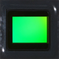
MT9P401I12STC Aptina LLC, MT9P401I12STC Datasheet - Page 37

MT9P401I12STC
Manufacturer Part Number
MT9P401I12STC
Description
SENSOR IMAGE CMOS 5MP 48LCC
Manufacturer
Aptina LLC
Type
CMOS Imagingr
Series
DigitalClarity®r
Specifications of MT9P401I12STC
Pixel Size
2.2µm x 2.2µm
Active Pixel Array
2592H x 1944V
Frames Per Second
60
Voltage - Supply
2.6 V ~ 3.1 V
Package / Case
48-iLCC
Sensor Image Color Type
Monochrome
Sensor Image Size
2592x1944Pixels
Operating Supply Voltage (typ)
1.8/2.8V
Operating Supply Voltage (max)
3.1V
Operating Temp Range
-30C to 70C
Package Type
ILCC
Operating Temperature Classification
Commercial
Mounting
Surface Mount
Pin Count
48
Lead Free Status / RoHS Status
Lead free / RoHS Compliant
Other names
557-1263
MT9P401I12STC
Q3412742
MT9P401I12STC
Q3412742
Available stocks
Company
Part Number
Manufacturer
Quantity
Price
Part Number:
MT9P401I12STC
Manufacturer:
APTINA
Quantity:
20 000
PLL-Generated Master Clock
Figure 13:
PLL Setup
PDF: 09005aef82acb06f/Source: 09005aef81a4a477
MT9P401_DS_2 - Rev. B 9/07 EN
PLL-Generated Master Clock
Note:
Note:
1. Bring the MT9P401 up as normal, make sure that
2. Set PLL_m_Factor, PLL_n_Divider, and PLL_p1_Divider based on the desired input
The D
should be captured on the falling edge of PIXCLK. The specific relationship of PIXCLK to
these other outputs can be adjusted in two ways. If Invert_Pixel_Clock is set, the sense of
PIXCLK is inverted from that shown in Figure 8 on page 13. In addition, if the pixel clock
has been divided by Divide_Pixel_Clock, it can be shifted relative to the other outputs by
setting Shift_Pixel_Clock.
The PLL contains a prescaler to divide the input clock applied on EXTCLK, a VCO to
multiply the prescaler output, and another divider stage to generate the output clock.
The clocking structure is shown in Figure 13. PLL control registers can be programmed
to generate desired master clock frequency.
EXTCLK
The MT9P401 has a PLL which can be used to generate the pixel clock internally.
To use the PLL:
f
where
M = PLL_m_Factor
N = PLL_n_Divider + 1
P1 = PLL_p1_Divider + 1
PIXCLK = (
The PLL control registers must be programmed while the sensor is in the software
Standby state. The effect of programming the PLL divisors while the sensor is in the
streaming state is undefined.
and then power on the PLL by setting Power_PLL (R0x10[0] = 1).
(
achieve the desired
If P1 is odd (that is, PLL_p1_Divider is even), the duty cycle of the internal system
clock will not be 50:50. In this case, it is important that either a slower clock is used or
all clock enable bits are set in R101.
f
EXTCLK) and output (
OUT
PLL_n_divider +1
, LV, FV, and STROBE outputs are launched on the rising edge of PIXCLK, and
f
EXTCLK × M) / (N × P1)
Micron Confidential and Proprietary
Pre PLL
(PFD)
Div
PLL Input Clock
N
f
PIXCLK using this formula:
f
PIXCLK) frequencies. Determine the M, N, and P1 values to
MT9P401: 1/2.5-Inch 5Mp Digital Image Sensor
PLL_m_factor
Multiplier
37
(VCO)
PLL
PLL Output Clock
M
Micron Technology, Inc., reserves the right to change products or specifications without notice.
PLL_p1_divider +1
Output
Div 1
PLL
P1
f
EXTCLK is between 6 and 27 MHz
©2007 Micron Technology, Inc. All rights reserved.
SYSCLK (PIXCLK)
Features


