ADUC7126BSTZ126-RL Analog Devices Inc, ADUC7126BSTZ126-RL Datasheet - Page 80
ADUC7126BSTZ126-RL
Manufacturer Part Number
ADUC7126BSTZ126-RL
Description
ARM7 With 12-Bit ADC & DACs, 128kB Flash
Manufacturer
Analog Devices Inc
Series
MicroConverter® ADuC7xxxr
Datasheet
1.ADUC7126BSTZ126.pdf
(104 pages)
Specifications of ADUC7126BSTZ126-RL
Core Processor
ARM7
Core Size
16/32-Bit
Speed
41.78MHz
Connectivity
EBI/EMI, I²C, SPI, UART/USART
Peripherals
POR, PWM, WDT
Number Of I /o
40
Program Memory Size
126KB (126K x 8)
Program Memory Type
FLASH
Ram Size
32K x 8
Voltage - Supply (vcc/vdd)
2.7 V ~ 3.6 V
Data Converters
A/D 12x12b, D/A 4x12b
Oscillator Type
Internal
Operating Temperature
-40°C ~ 125°C
Package / Case
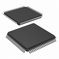
80-LQFP
Lead Free Status / RoHS Status
Lead free / RoHS Compliant
Eeprom Size
-
Lead Free Status / RoHS Status
Lead free / RoHS Compliant
Available stocks
Company
Part Number
Manufacturer
Quantity
Price
Company:

Part Number:
ADUC7126BSTZ126-RL
Manufacturer:
Analog Devices Inc
Quantity:
10 000


ADuC7124/ADuC7126
Table 114. PWM Output Selection, HMODE = 1
ENA
0
X
1
1
1
1
1
2
On power-up, PWMCON0 defaults to 0x12 (HOFF = 1 and
HMODE = 1). All GPIO pins associated with the PWM are
configured in PWM mode by default (see Table 115).
Table 115. Compare Registers
Name
PWM0COM0
PWM0COM1
PWM0COM2
PWM1COM0
PWM1COM1
PWM1COM2
PWM2COM0
PWM2COM1
PWM2COM2
The PWM trip interrupt can be cleared by writing any value to
the PWMCLRI MMR. Note that, when using the PWM trip
interrupt, users should make sure that the PWM interrupt
has been cleared before exiting the ISR. This prevents
generation of multiple interrupts.
PWM Convert Start Control
The PWM can be configured to generate an ADC convert start
signal after the active low side signal goes high. There is a
programmable delay between the time that the low-side signal
goes high and the convert start signal is generated.
This is controlled via the PWMCON1 MMR. If the delay
selected is higher than the width of the PWM pulse, the
interrupt remains low.
X = don’t care.
HS = high side, LS = low side.
PWMCON0 MMR
HOFF
0
1
0
0
0
0
POINV
X
X
0
0
1
1
Address
0xFFFF0F84
0xFFFF0F88
0xFFFF0F8C
0xFFFF0F94
0xFFFF0F98
0xFFFF0F9C
0xFFFF0FA4
0xFFFF0FA8
0xFFFF0FAC
1
DIR
X
X
0
1
0
1
PWM0
1
1
0
HS
HS
1
Default Value
0x0000
0x0000
0x0000
0x0000
0x0000
0x0000
0x0000
0x0000
0x0000
PWM1
1
0
0
LS
LS
1
PWM Outputs
PWM2
1
1
HS
0
1
HS
2
Access
R/W
R/W
R/W
R/W
R/W
R/W
R/W
R/W
R/W
PWM3
1
0
LS
0
1
LS
Rev. B | Page 80 of 104
Table 116. PWMCON1 MMR Bit Descriptions (Address =
0xFFFF0FB4; Default Value = 0x00)
Bit
7
[3:0]
When calculating the time from the convert start delay to the
start of an ADC conversion, the user must take account of
internal delays. The following example shows the case of a delay
of four clocks. One additional clock is required to pass the
convert start signal to the ADC logic. Once the ADC logic
receives the convert start signal, an ADC conversion begins on
the next ADC clock edge (see Figure 50).
SIGNAL PASSED
TO ADC LOGIC
PWM SIGNAL
TO CONVST
LOW SIDE
Value
0000
0001
0010
0011
0100
0101
0110
0111
1000
1001
1010
1011
1100
1101
1110
1111
COUNT
UCLK
Name
CSEN
CSD3
CSD2
CSD1
CSD0
Figure 50. ADC Conversion
Description
Set to 1 by the user to enable the PWM
to generate a convert start signal.
Cleared by user to disable the PWM
convert start signal.
Convert start delay. Delays the convert
start signal by a number of clock
pulses.
Four clock pulses.
Eight clock pulses.
12 clock pulses.
16 clock pulses.
20 clock pulses.
24 clock pulses.
28 clock pulses.
32 clock pulses.
36 clock pulses.
40 clock pulses.
44 clock pulses.
48 clock pulses.
52 clock pulses.
56 clock pulses.
60 clock pulses.
64 clock pulses.
Related parts for ADUC7126BSTZ126-RL
Image
Part Number
Description
Manufacturer
Datasheet
Request
R

Part Number:
Description:
Precision Analog Microcontroller, 12-Bit Analog I/O, Large Memory, ARM7TDMI MCU with Enhanced IRQ Handler
Manufacturer:
Analog Devices
Datasheet:

Part Number:
Description:
±1.7g Dual-Axis IMEMS Accelerometer Evaluation Board
Manufacturer:
Analog Devices Inc
Datasheet:

Part Number:
Description:
Inertial Sensor Evaluation System
Manufacturer:
Analog Devices Inc
Datasheet:
Part Number:
Description:
Manufacturer:
Analog Devices Inc
Datasheet:
Part Number:
Description:
Manufacturer:
Analog Devices Inc
Datasheet:
Part Number:
Description:
Manufacturer:
Analog Devices Inc
Datasheet:
Part Number:
Description:
Manufacturer:
Analog Devices Inc
Datasheet:
Part Number:
Description:
Manufacturer:
Analog Devices Inc
Datasheet:
Part Number:
Description:
Manufacturer:
Analog Devices Inc
Datasheet:
Part Number:
Description:
Manufacturer:
Analog Devices Inc
Datasheet:
Part Number:
Description:
Manufacturer:
Analog Devices Inc
Datasheet:
Part Number:
Description:
Manufacturer:
Analog Devices Inc
Datasheet:
Part Number:
Description:
Manufacturer:
Analog Devices Inc
Datasheet: