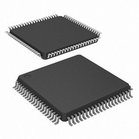
ADUC7126BSTZ126-RL Analog Devices Inc, ADUC7126BSTZ126-RL Datasheet - Page 14

ADUC7126BSTZ126-RL
Manufacturer Part Number
ADUC7126BSTZ126-RL
Description
ARM7 With 12-Bit ADC & DACs, 128kB Flash
Manufacturer
Analog Devices Inc
Series
MicroConverter® ADuC7xxxr
Datasheet
1.ADUC7126BSTZ126.pdf
(104 pages)
Specifications of ADUC7126BSTZ126-RL
Core Processor
ARM7
Core Size
16/32-Bit
Speed
41.78MHz
Connectivity
EBI/EMI, I²C, SPI, UART/USART
Peripherals
POR, PWM, WDT
Number Of I /o
40
Program Memory Size
126KB (126K x 8)
Program Memory Type
FLASH
Ram Size
32K x 8
Voltage - Supply (vcc/vdd)
2.7 V ~ 3.6 V
Data Converters
A/D 12x12b, D/A 4x12b
Oscillator Type
Internal
Operating Temperature
-40°C ~ 125°C
Package / Case
80-LQFP
Lead Free Status / RoHS Status
Lead free / RoHS Compliant
Eeprom Size
-
Lead Free Status / RoHS Status
Lead free / RoHS Compliant
Available stocks
Company
Part Number
Manufacturer
Quantity
Price
Company:
Part Number:
ADUC7126BSTZ126-RL
Manufacturer:
Analog Devices Inc
Quantity:
10 000
ADuC7124/ADuC7126
PIN CONFIGURATIONS AND FUNCTION DESCRIPTIONS
Table 9. Pin Function Descriptions (ADuC7124 64-Lead LFCSP)
Pin No.
0
1
2
3
4
5
6
7
8
9
10
11
12
13
Mnemonic
Exposed Paddle
ADC4
ADC5
ADC6
ADC7
ADC8
ADC9
ADCNEG
DACGND
DACV
DAC0/ADC12
DAC1/ADC13
TMS
TDI
DD
NOTES
1. THE EXPOSED PADDLE MUST BE SOLDERED TO THE PCB TO ENSURE PROPER
BM/P0.0/CMP
HEAT DISSIPATION, NOISE, AND MECHANICAL STRENGTH BENEFITS.
DAC0/ADC12
DAC1/ADC13
NC = NO CONNECT
OUT
ADCNEG
DACGND
DACV
/PLAI[7]
XCLKO
XCLKI
ADC4
ADC5
ADC6
ADC7
ADC8
ADC9
TMS
TDI
DD
10
11
12
13
14
15
16
1
2
3
4
5
6
7
8
9
PIN 1
INDICATOR
Description
Exposed Paddle. The LFCSP_VQ has an exposed paddle that must be left unconnected.
Single-Ended or Differential Analog Input 4.
Single-Ended or Differential Analog Input 5.
Single-Ended or Differential Analog Input 6.
Single-Ended or Differential Analog Input 7.
Single-Ended or Differential Analog Input 8.
Single-Ended or Differential Analog Input 9.
Bias Point or Negative Analog Input of the ADC in Pseudo Differential Mode. Must be
connected to the ground of the signal to convert. This bias point must be between 0 V
and 1 V.
Ground for the DAC. Typically connected to AGND.
3.3 V Power Supply for the DACs. Must be connected to AV
DAC0 Voltage Output (DAC0).
Single-Ended or Differential Analog Input 12 (ADC12).
DAC1 Voltage Output (DAC1).
Single-Ended or Differential Analog Input 13 (ADC13).
JTAG Test Port Input, Test Mode Select. Debug and download access.
JTAG Test Port Input, Test Data In.
Figure 7. ADuC7124 Pin Configuration
ADuC7124
(Not to Scale)
TOP VIEW
Rev. B | Page 14 of 104
48
47
46
45
44
43
42
41
40
39
38
37
36
35
34
33
P1.3/SPM3/CTS/I2C1SDA/PLAI[3]
P1.4/SPM4/RI/SPICLK/PLAI[4]/IRQ2
P1.5/SPM5/DCD/SPIMISO/PLAI[5]/IRQ3
P4.1/PLAO[9]/SOUT1
P4.0/PLAO[8]/SIN1
P1.6/SPM6/PLAI[6]
P1.7/SPM7/DTR/SPICS/PLAO[0]
P3.7/PWM
P3.6/PWM
IOV
IOGND
P0.7/ECLK/XCLK/SPM8/PLAO[4]/SIN0
P2.0/SPM9/PLAO[5]/CONV
IRQ1/P0.5/ADC
IRQ0/P0.4/PWM
RST
DD
SYNC
TRIP
/PLAI[14]
/PLAI[15]
BUSY
TRIP
/PLAO[1]
/PLAO[2]
START
/SOUT0
DD
.


