ADUC7126BSTZ126-RL Analog Devices Inc, ADUC7126BSTZ126-RL Datasheet - Page 63
ADUC7126BSTZ126-RL
Manufacturer Part Number
ADUC7126BSTZ126-RL
Description
ARM7 With 12-Bit ADC & DACs, 128kB Flash
Manufacturer
Analog Devices Inc
Series
MicroConverter® ADuC7xxxr
Datasheet
1.ADUC7126BSTZ126.pdf
(104 pages)
Specifications of ADUC7126BSTZ126-RL
Core Processor
ARM7
Core Size
16/32-Bit
Speed
41.78MHz
Connectivity
EBI/EMI, I²C, SPI, UART/USART
Peripherals
POR, PWM, WDT
Number Of I /o
40
Program Memory Size
126KB (126K x 8)
Program Memory Type
FLASH
Ram Size
32K x 8
Voltage - Supply (vcc/vdd)
2.7 V ~ 3.6 V
Data Converters
A/D 12x12b, D/A 4x12b
Oscillator Type
Internal
Operating Temperature
-40°C ~ 125°C
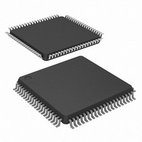
Package / Case
80-LQFP
Lead Free Status / RoHS Status
Lead free / RoHS Compliant
Eeprom Size
-
Lead Free Status / RoHS Status
Lead free / RoHS Compliant
Available stocks
Company
Part Number
Manufacturer
Quantity
Price
Company:

Part Number:
ADUC7126BSTZ126-RL
Manufacturer:
Analog Devices Inc
Quantity:
10 000


Table 93. COMxIID0 MMR Bit Descriptions
Bit
[7:6]
[5:4]
[3:1]
0
1
COM0FCR Register
Name:
Address:
Default Value:
Access:
The FIFO control register (FCR) is a write-only register at the
same address as the interrupt identification register (IIR), which
is a read-only register.
A frame time is the time allotted for one start bit, n data bits, one parity bit,
and one stop bit. Here, n is the word length selected with the WLS bits in
COMxCON0.
WLS[1:0] = 00: timeout threshold = time for 32 bits = (1 + 5 + 1 + 1) × 4.
WLS[1:0] = 01: timeout threshold = time for 36 bits = (1 + 6 + 1 + 1) × 4.
WLS[1:0] = 10: timeout threshold = time for 40 bits = (1 + 7 + 1 + 1) × 4.
WLS[1:0] = 11: timeout threshold = time for 44 bits = (1 + 8 + 1 + 1) × 4.
Name
FIFOMODE
Reserved
STATUS[2:0]
NINT
Description
0x0: non-FIFO mode.
0x1: reserved.
0x2: reserved.
0x3: FIFO mode. Set automatically if
FIFOEN is set.
Interrupt status bits that work only when
NINT is set.
[000]: modem status interrupt. Cleared by
reading COMxSTA1. Priority 4.
[001]: for non-FIFO mode, transmit buffer
empty interrupt.
For FIFO mode, Tx FIFO is empty.
Cleared by writing COMxTX or reading
COMxIID0. Priority 3.
[010]: non-FIFO mode. Receive buffer data
ready interrupt. Cleared automatically by
reading COMxRX.
For FIFO mode, set trigger level reached.
Cleared automatically when FIFO drops
below the trigger level. Priority 2.
[011]: receive line status error interrupt.
Cleared by reading COMxSTA0. Priority 1.
[110]: Rx FIFO timeout interrupt (FIFO
mode only). Set automatically if there is at
least one byte in the Rx FIFO, and there is
no access to the Rx FIFO in the next four-
frames accessing cycle. Cleared by reading
COMxRX, setting RXRST, or when a new
byte arrives in the Rx FIFO
[Other state]: reserved.
Set to disable interrupt flags by
STATUS[2:0]. Clear to enable interrupt.
FIFO mode flag.
COM0FCR
0xFFFF0708
0x00
Read/write
1
. Priority 2.
Rev. B | Page 63 of 104
COM1FCR Register
Name:
Address:
Default Value:
Access:
The FIFO control register (FCR) is a write-only register at the
same address as the interrupt identification register (IIR), which
is a read-only register.
Table 94. COMxFCR MMR Bit Descriptions
Bit
[7:5]
[4:3]
2
1
0
COM0CON0 Register
Name:
Address:
Default Value:
Access:
COM0CON0 is the line control register for UART0.
Name
RXFIFOTL
Reserved
TXRST
RXRST
FIFOEN
Description
Receiver FIFO trigger level. RXFIFOTL sets the
trigger level for the receiver FIFO. When the
trigger level is reached, a receiver data-ready
interrupt is generated (if the interrupt
request is enabled). When the FIFO drops
below the trigger level, the interrupt is
cleared.
0x0: one byte.
0x1: two bytes.
0x2: four bytes.
0x3: six bytes.
0x4: eight bytes.
0x5: 10 bytes.
0x6: 12 bytes.
0x7: 14 bytes.
Tx FIFO reset. Writing a 1 flushes the Tx FIFO.
Does not affect shift register. Note that
TXRST should be cleared manually to make
Tx FIFO work after flushing.
Rx FIFO reset. Writing a 1 flushes the Rx FIFO.
Does not affect shift register. Note that
RXRST should be cleared manually to make
the Rx FIFO work after flushing.
Transmitter and receiver FIFOs mode enable.
FIFOEN must be set before other FCR bits are
written to. Set for FIFO mode. The transmitter
and receiver FIFOs are enabled. Cleared for
non-FIFO mode; the transmitter and receiver
FIFOs are disabled, and the FIFO pointers are
cleared.
ADuC7124/ADuC7126
COM0CON0
0xFFFF070C
0x00
Read/write
COM1FCR
0xFFFF0748
0x00
Read/write
Related parts for ADUC7126BSTZ126-RL
Image
Part Number
Description
Manufacturer
Datasheet
Request
R

Part Number:
Description:
Precision Analog Microcontroller, 12-Bit Analog I/O, Large Memory, ARM7TDMI MCU with Enhanced IRQ Handler
Manufacturer:
Analog Devices
Datasheet:

Part Number:
Description:
±1.7g Dual-Axis IMEMS Accelerometer Evaluation Board
Manufacturer:
Analog Devices Inc
Datasheet:

Part Number:
Description:
Inertial Sensor Evaluation System
Manufacturer:
Analog Devices Inc
Datasheet:
Part Number:
Description:
Manufacturer:
Analog Devices Inc
Datasheet:
Part Number:
Description:
Manufacturer:
Analog Devices Inc
Datasheet:
Part Number:
Description:
Manufacturer:
Analog Devices Inc
Datasheet:
Part Number:
Description:
Manufacturer:
Analog Devices Inc
Datasheet:
Part Number:
Description:
Manufacturer:
Analog Devices Inc
Datasheet:
Part Number:
Description:
Manufacturer:
Analog Devices Inc
Datasheet:
Part Number:
Description:
Manufacturer:
Analog Devices Inc
Datasheet:
Part Number:
Description:
Manufacturer:
Analog Devices Inc
Datasheet:
Part Number:
Description:
Manufacturer:
Analog Devices Inc
Datasheet:
Part Number:
Description:
Manufacturer:
Analog Devices Inc
Datasheet: