ADUC7126BSTZ126-RL Analog Devices Inc, ADUC7126BSTZ126-RL Datasheet - Page 17
ADUC7126BSTZ126-RL
Manufacturer Part Number
ADUC7126BSTZ126-RL
Description
ARM7 With 12-Bit ADC & DACs, 128kB Flash
Manufacturer
Analog Devices Inc
Series
MicroConverter® ADuC7xxxr
Datasheet
1.ADUC7126BSTZ126.pdf
(104 pages)
Specifications of ADUC7126BSTZ126-RL
Core Processor
ARM7
Core Size
16/32-Bit
Speed
41.78MHz
Connectivity
EBI/EMI, I²C, SPI, UART/USART
Peripherals
POR, PWM, WDT
Number Of I /o
40
Program Memory Size
126KB (126K x 8)
Program Memory Type
FLASH
Ram Size
32K x 8
Voltage - Supply (vcc/vdd)
2.7 V ~ 3.6 V
Data Converters
A/D 12x12b, D/A 4x12b
Oscillator Type
Internal
Operating Temperature
-40°C ~ 125°C
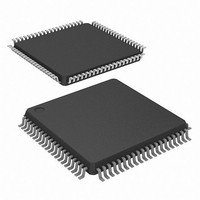
Package / Case
80-LQFP
Lead Free Status / RoHS Status
Lead free / RoHS Compliant
Eeprom Size
-
Lead Free Status / RoHS Status
Lead free / RoHS Compliant
Available stocks
Company
Part Number
Manufacturer
Quantity
Price
Company:

Part Number:
ADUC7126BSTZ126-RL
Manufacturer:
Analog Devices Inc
Quantity:
10 000


Pin No.
50
51
52
53
54
55
56
57
58
59
60
61
62
63
64
Mnemonic
P1.1/SPM1/SOUT0/I2C0SDA/PLAI[1]
P1.0/T1/SPM0/SIN0/I2C0SCL/PLAI[0]
P4.2/PLAO[10]
P4.3/PLAO[11]
P4.4/PLAO[12]
RTCK
V
DAC
AV
AGND
GND
ADC0
ADC1
ADC2/CMP0
ADC3/CMP1
REF
DD
REF
REF
Description
General-Purpose Input and Output Port 1.1 (P1.1).
Serial Port Multiplexed (SPM1).
UART0 Output (SOUT0).
I2C0 (I2C0SDA).
Programmable Logic Array Input Element 1 (PLAI[1]).
General-Purpose Input and Output Port 1.0 (P1.0).
Timer1 Input (T1).
Serial Port Multiplexed (SPM0).
UART0 Input (SIN0).
I2C0 (I2C0SCL).
Programmable Logic Array Input Element 0 (PLAI[0]).
General-Purpose Input and Output Port 4.2 (P4.2).
Programmable Logic Array Output Element 10 (PLAO[10]).
General-Purpose Input and Output Port 4.3 (P4.3).
Programmable Logic Array Output Element 11 (PLAO[11]).
General-Purpose Input and Output Port 4.4 (P4.4).
Programmable Logic Array Output Element 12 (PLAO[12]).
JTAG Test Port Output, JTAG Return Test Clock.
2.5 V Internal Voltage Reference. Must be connected to a 0.47 µF capacitor when using
the internal reference.
External Voltage Reference for the DACs. Range: DACGND to DACV
3.3 V Analog Power.
Analog Ground. Ground reference point for the analog circuitry.
Ground Voltage Reference for the ADC. For optimal performance, the analog power
supply should be separated from IOGND and DGND.
Single-Ended or Differential Analog Input 0.
Single-Ended or Differential Analog Input 1.
Single-Ended or Differential Analog Input 2 (ADC2).
Comparator Positive Input (CMP0).
Single-Ended or Differential Analog Input 3 (ADC3).
Comparator Negative Input (CMP1).
Rev. B | Page 17 of 104
ADuC7124/ADuC7126
DD
.
Related parts for ADUC7126BSTZ126-RL
Image
Part Number
Description
Manufacturer
Datasheet
Request
R

Part Number:
Description:
Precision Analog Microcontroller, 12-Bit Analog I/O, Large Memory, ARM7TDMI MCU with Enhanced IRQ Handler
Manufacturer:
Analog Devices
Datasheet:

Part Number:
Description:
±1.7g Dual-Axis IMEMS Accelerometer Evaluation Board
Manufacturer:
Analog Devices Inc
Datasheet:

Part Number:
Description:
Inertial Sensor Evaluation System
Manufacturer:
Analog Devices Inc
Datasheet:
Part Number:
Description:
Manufacturer:
Analog Devices Inc
Datasheet:
Part Number:
Description:
Manufacturer:
Analog Devices Inc
Datasheet:
Part Number:
Description:
Manufacturer:
Analog Devices Inc
Datasheet:
Part Number:
Description:
Manufacturer:
Analog Devices Inc
Datasheet:
Part Number:
Description:
Manufacturer:
Analog Devices Inc
Datasheet:
Part Number:
Description:
Manufacturer:
Analog Devices Inc
Datasheet:
Part Number:
Description:
Manufacturer:
Analog Devices Inc
Datasheet:
Part Number:
Description:
Manufacturer:
Analog Devices Inc
Datasheet:
Part Number:
Description:
Manufacturer:
Analog Devices Inc
Datasheet:
Part Number:
Description:
Manufacturer:
Analog Devices Inc
Datasheet: