ADUC7126BSTZ126-RL Analog Devices Inc, ADUC7126BSTZ126-RL Datasheet - Page 49
ADUC7126BSTZ126-RL
Manufacturer Part Number
ADUC7126BSTZ126-RL
Description
ARM7 With 12-Bit ADC & DACs, 128kB Flash
Manufacturer
Analog Devices Inc
Series
MicroConverter® ADuC7xxxr
Datasheet
1.ADUC7126BSTZ126.pdf
(104 pages)
Specifications of ADUC7126BSTZ126-RL
Core Processor
ARM7
Core Size
16/32-Bit
Speed
41.78MHz
Connectivity
EBI/EMI, I²C, SPI, UART/USART
Peripherals
POR, PWM, WDT
Number Of I /o
40
Program Memory Size
126KB (126K x 8)
Program Memory Type
FLASH
Ram Size
32K x 8
Voltage - Supply (vcc/vdd)
2.7 V ~ 3.6 V
Data Converters
A/D 12x12b, D/A 4x12b
Oscillator Type
Internal
Operating Temperature
-40°C ~ 125°C
Package / Case
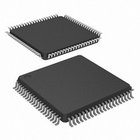
80-LQFP
Lead Free Status / RoHS Status
Lead free / RoHS Compliant
Eeprom Size
-
Lead Free Status / RoHS Status
Lead free / RoHS Compliant
Available stocks
Company
Part Number
Manufacturer
Quantity
Price
Company:

Part Number:
ADUC7126BSTZ126-RL
Manufacturer:
Analog Devices Inc
Quantity:
10 000


Table 59. REMAP MMR Bit Descriptions
(Address = 0xFFFF0220. Default Value = 0x00)
Bit
0
Remap Operation
When a reset occurs on the ADuC7124/ADuC7126, execution
automatically starts in factory programmed, internal
configuration code. This kernel is hidden and cannot be accessed
by user code. If the part is in normal mode (BM pin is high), it
executes the power-on configuration routine of the kernel and
then jumps to the reset vector address, 0x00000000, to execute
the reset exception routine of the user.
Because the Flash/EE is mirrored at the bottom of the memory
array at reset, the reset interrupt routine must always be written
in Flash/EE.
The remap is done from Flash/EE by setting Bit 0 of the REMAP
register. Caution must be taken to execute this command from
Flash/EE, above Address 0x00080020, and not from the bottom
of the array, because this is replaced by the SRAM.
This operation is reversible. The Flash/EE can be remapped at
Address 0x00000000 by clearing Bit 0 of the REMAP MMR.
Caution must again be taken to execute the remap function
from outside the mirrored area. Any type of reset remaps the
Flash/EE memory at the bottom of the array.
Reset Operation
There are four kinds of reset: external, power-on, watchdog
expiation, and software force. The RSTSTA register indicates
the source of the last reset, and RSTCLR allows clearing of the
RSTSTA register. These registers can be used during a reset
exception service routine to identify the source of the reset.
If RSTSTA is null, the reset is external.
The RSTCFG register allows different peripherals to retain their
state after a watchdog or software reset.
RSTSTA Register
Name:
Address:
Default Value:
Access:
Name
Remap
Description
Remap bit.
Set by the user to remap the SRAM to Address
0x00000000.
Cleared automatically after reset to remap the
Flash/EE memory to Address 0x00000000.
RSTSTA
0xFFFF0230
0x01
Read only
Rev. B | Page 49 of 104
Table 60. RSTSTA MMR Bit Descriptions
Bit
[7:3]
2
1
0
RSTCLR Register
Name:
Address:
Default Value:
Access:
Note that to clear the RSTSTA register, users must write the
Value 0x07 to the RSTCLR register.
RSTCFG Register
Name:
Address:
Default Value:
Access:
Table 61. RSTCFG MMR Bit Descriptions
Bit
[7:3]
2
1
0
The RSTCFG write sequence is as follows:
1.
2.
3.
Write Code 0x76 to Register RSTKEY1.
Write user value to Register RSTCFG.
Write Code 0xB1 to Register RSTKEY2.
Description
Reserved.
Software reset.
Set by the user to force a software reset.
Cleared by setting the corresponding bit in RSTCLR.
Watchdog timeout.
Set automatically when a watchdog timeout occurs.
Cleared by setting the corresponding bit in RSTCLR.
Power-on reset.
Set automatically when a power-on reset occurs.
Cleared by setting the corresponding bit in RSTCLR.
Description
Reserved. Always set to 0.
This bit is set to 1 to configure the DAC outputs to
retain their state after a watchdog or software reset.
This bit is cleared for the DAC pins and registers to
return to their default state.
Reserved. Always set to 0.
This bit is set to 1 to configure the GPIO pins to retain
their state after a watchdog or software reset.
This bit is cleared for the GPIO pins and registers to
return to their default state.
RSTCLR
0xFFFF0234
0x00
Write only
RSTCFG
0xFFFF024C
0x05
Read/write
ADuC7124/ADuC7126
Related parts for ADUC7126BSTZ126-RL
Image
Part Number
Description
Manufacturer
Datasheet
Request
R

Part Number:
Description:
Precision Analog Microcontroller, 12-Bit Analog I/O, Large Memory, ARM7TDMI MCU with Enhanced IRQ Handler
Manufacturer:
Analog Devices
Datasheet:

Part Number:
Description:
±1.7g Dual-Axis IMEMS Accelerometer Evaluation Board
Manufacturer:
Analog Devices Inc
Datasheet:

Part Number:
Description:
Inertial Sensor Evaluation System
Manufacturer:
Analog Devices Inc
Datasheet:
Part Number:
Description:
Manufacturer:
Analog Devices Inc
Datasheet:
Part Number:
Description:
Manufacturer:
Analog Devices Inc
Datasheet:
Part Number:
Description:
Manufacturer:
Analog Devices Inc
Datasheet:
Part Number:
Description:
Manufacturer:
Analog Devices Inc
Datasheet:
Part Number:
Description:
Manufacturer:
Analog Devices Inc
Datasheet:
Part Number:
Description:
Manufacturer:
Analog Devices Inc
Datasheet:
Part Number:
Description:
Manufacturer:
Analog Devices Inc
Datasheet:
Part Number:
Description:
Manufacturer:
Analog Devices Inc
Datasheet:
Part Number:
Description:
Manufacturer:
Analog Devices Inc
Datasheet:
Part Number:
Description:
Manufacturer:
Analog Devices Inc
Datasheet: