ADUC7126BSTZ126-RL Analog Devices Inc, ADUC7126BSTZ126-RL Datasheet - Page 59
ADUC7126BSTZ126-RL
Manufacturer Part Number
ADUC7126BSTZ126-RL
Description
ARM7 With 12-Bit ADC & DACs, 128kB Flash
Manufacturer
Analog Devices Inc
Series
MicroConverter® ADuC7xxxr
Datasheet
1.ADUC7126BSTZ126.pdf
(104 pages)
Specifications of ADUC7126BSTZ126-RL
Core Processor
ARM7
Core Size
16/32-Bit
Speed
41.78MHz
Connectivity
EBI/EMI, I²C, SPI, UART/USART
Peripherals
POR, PWM, WDT
Number Of I /o
40
Program Memory Size
126KB (126K x 8)
Program Memory Type
FLASH
Ram Size
32K x 8
Voltage - Supply (vcc/vdd)
2.7 V ~ 3.6 V
Data Converters
A/D 12x12b, D/A 4x12b
Oscillator Type
Internal
Operating Temperature
-40°C ~ 125°C
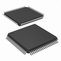
Package / Case
80-LQFP
Lead Free Status / RoHS Status
Lead free / RoHS Compliant
Eeprom Size
-
Lead Free Status / RoHS Status
Lead free / RoHS Compliant
Available stocks
Company
Part Number
Manufacturer
Quantity
Price
Company:

Part Number:
ADUC7126BSTZ126-RL
Manufacturer:
Analog Devices Inc
Quantity:
10 000


Table 79. GPxCON Registers
Name
GP0CON
GP1CON
GP2CON
GP3CON
GP4CON
GPxCON are the Port x control registers that select the function
of each pin of Port x, as described in Table 80.
Table 80. GPxCON MMR Bit Descriptions
Bit
[31:30]
[29:28]
[27:26]
[25:24]
[23:22]
[21:20]
[19:18]
[17:16]
[15:14]
[13:12]
[11:10]
[9:8]
[7:6]
[5:4]
[3:2]
[1:0]
Table 81. GPxPAR Registers
Name
GP0PAR
GP1PAR
GP2PAR
GP3PAR
GP4PAR
The GPxPAR registers program the parameters for Port 0, Port 1,
Port 2, Port 3, and Port 4. Note that the GPxDAT MMR must
always be written after changing the GPxPAR MMR.
Table 82. GPxPAR MMR Bit Descriptions
Bit
31
[30:29]
28
27
[26:25]
24
23
[22:21]
20
19
[18:17]
Description
Reserved.
Select function of Px.7 pin.
Reserved.
Select function of Px.6 pin.
Reserved.
Select function of Px.5 pin.
Reserved.
Select function of Px.4 pin.
Reserved.
Select function of Px.3 pin.
Reserved.
Select function of Px.2 pin.
Reserved.
Select function of Px.1 pin.
Reserved.
Select function of Px.0 pin.
Address
0xFFFFF400
0xFFFFF404
0xFFFFF408
0xFFFFF40C
0xFFFFF410
Address
0xFFFFF42C
0xFFFFF43C
0xFFFFF44C
0xFFFFF45C
0xFFFFF46C
Description
Reserved.
Drive strength Px.7.
Pull-up disable Px.7.
Reserved.
Drive strength Px.6.
Pull-up disable Px.6.
Reserved.
Drive strength Px.5.
Pull-up disable Px.5.
Reserved.
Drive strength Px.4.
Default Value
0x00000000
0x00000000
0x00000000
0x00000000
0x00000000
Default Value
0x20000000
0x00000000
0x000000FF
0x00222222
0x00000000
Access
R/W
R/W
R/W
R/W
R/W
Access
R/W
R/W
R/W
R/W
R/W
Rev. B | Page 59 of 104
Bit
16
15
[14:13]
12
11
[10:9]
8
7
[6:5]
4
3
[2:1]
0
Table 83. GPIO Drive Strength Control Bits Descriptions
Control Bits Value
00
01
1x
–0.1
–0.2
–0.3
–0.4
3.6
3.4
3.2
3.0
2.8
2.6
2.4
2.2
2.0
0.5
0.4
0.3
0.2
0.1
–24
–24
0
Figure 46. Programmable Strength for High Level
Figure 47. Programmable Strength for Low Level
–18
–18
HIGH DRIVE STRENGTH
MEDIUM DRIVE STRENGTH
LOW DRIVE STRENGTH
HIGH DRIVE STRENGTH
MEDIUM DRIVE STRENGTH
LOW DRIVE STRENGTH
Description
Pull-up disable Px.4.
Reserved.
Drive strength Px.3.
Pull-up disable Px.3.
Reserved.
Drive strength Px.2.
Pull-up disable Px.2.
Reserved.
Drive strength Px.1.
Pull-up disable Px.1.
Reserved.
Drive strength Px.0.
Pull-up disable Px.0.
–12
–12
SINK/SOURCE CURRENT (mA)
SINK/SOURCE CURRENT (mA)
Description
Medium drive strength.
Low drive strength.
High drive strength.
–6
–6
ADuC7124/ADuC7126
0
0
6
6
12
12
18
18
24
24
Related parts for ADUC7126BSTZ126-RL
Image
Part Number
Description
Manufacturer
Datasheet
Request
R

Part Number:
Description:
Precision Analog Microcontroller, 12-Bit Analog I/O, Large Memory, ARM7TDMI MCU with Enhanced IRQ Handler
Manufacturer:
Analog Devices
Datasheet:

Part Number:
Description:
±1.7g Dual-Axis IMEMS Accelerometer Evaluation Board
Manufacturer:
Analog Devices Inc
Datasheet:

Part Number:
Description:
Inertial Sensor Evaluation System
Manufacturer:
Analog Devices Inc
Datasheet:
Part Number:
Description:
Manufacturer:
Analog Devices Inc
Datasheet:
Part Number:
Description:
Manufacturer:
Analog Devices Inc
Datasheet:
Part Number:
Description:
Manufacturer:
Analog Devices Inc
Datasheet:
Part Number:
Description:
Manufacturer:
Analog Devices Inc
Datasheet:
Part Number:
Description:
Manufacturer:
Analog Devices Inc
Datasheet:
Part Number:
Description:
Manufacturer:
Analog Devices Inc
Datasheet:
Part Number:
Description:
Manufacturer:
Analog Devices Inc
Datasheet:
Part Number:
Description:
Manufacturer:
Analog Devices Inc
Datasheet:
Part Number:
Description:
Manufacturer:
Analog Devices Inc
Datasheet:
Part Number:
Description:
Manufacturer:
Analog Devices Inc
Datasheet: