ADUC7126BSTZ126-RL Analog Devices Inc, ADUC7126BSTZ126-RL Datasheet - Page 66
ADUC7126BSTZ126-RL
Manufacturer Part Number
ADUC7126BSTZ126-RL
Description
ARM7 With 12-Bit ADC & DACs, 128kB Flash
Manufacturer
Analog Devices Inc
Series
MicroConverter® ADuC7xxxr
Datasheet
1.ADUC7126BSTZ126.pdf
(104 pages)
Specifications of ADUC7126BSTZ126-RL
Core Processor
ARM7
Core Size
16/32-Bit
Speed
41.78MHz
Connectivity
EBI/EMI, I²C, SPI, UART/USART
Peripherals
POR, PWM, WDT
Number Of I /o
40
Program Memory Size
126KB (126K x 8)
Program Memory Type
FLASH
Ram Size
32K x 8
Voltage - Supply (vcc/vdd)
2.7 V ~ 3.6 V
Data Converters
A/D 12x12b, D/A 4x12b
Oscillator Type
Internal
Operating Temperature
-40°C ~ 125°C
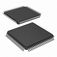
Package / Case
80-LQFP
Lead Free Status / RoHS Status
Lead free / RoHS Compliant
Eeprom Size
-
Lead Free Status / RoHS Status
Lead free / RoHS Compliant
Available stocks
Company
Part Number
Manufacturer
Quantity
Price
Company:

Part Number:
ADUC7126BSTZ126-RL
Manufacturer:
Analog Devices Inc
Quantity:
10 000


ADuC7124/ADuC7126
COM0DIV2 Register
Name:
Address:
Default Value:
Access:
COM0DIV2 is a 16-bit fractional baud divide register for
UART0.
COM1DIV2 Register
Name:
Address:
Default Value:
Access:
COM1DIV2 is a 16-bit fractional baud divide register for UART1.
Table 99. COMxDIV2 MMR Bit Descriptions
Bit
15
[14:13]
[12:11]
[10:0]
SERIAL PERIPHERAL INTERFACE
The ADuC7124/ADuC7126 integrate a complete hardware serial
peripheral interface (SPI) on chip. SPI is an industry standard,
synchronous serial interface that allows eight bits of data to be
synchronously transmitted and simultaneously received, that is,
full duplex up to a maximum bit rate of 20 Mbps.
The SPI port can be configured for master or slave operation
and typically consists of four pins: MISO, MOSI, CLK, and CS
MISO (Master In, Slave Out) Pin
The MISO pin is configured as an input line in master mode
and an output line in slave mode. The MISO line on the master
(data in) should be connected to the MISO line in the slave
device (data out). The data is transferred as byte wide (8-bit)
serial data, MSB first.
Name
FBEN
FBM[1:0]
FBN[10:0]
Description
Fractional baud rate generator enable bit.
Set by the user to enable the fractional
baud rate generator.
Cleared by the user to generate the baud
rate using the standard 450 UART baud
rate generator.
Reserved.
M if FBM = 0, M = 4 (see The Fractional
Divider section).
N (see The Fractional Divider section).
COM0DIV2
0xFFFF072C
0x0000
Read/write
COM1DIV2
0xFFFF076C
0x0000
Read/write
Rev. B | Page 66 of 104
.
MOSI (Master Out, Slave In) Pin
The MOSI pin is configured as an output line in master mode
and an input line in slave mode. The MOSI line on the master
(data out) should be connected to the MOSI line in the slave
device (data in). The data is transferred as byte wide (8-bit)
serial data, MSB first.
CLK (Serial Clock I/O) Pin
The master serial clock (CLK) synchronizes the data being
transmitted and received through the MOSI CLK period.
Therefore, a byte is transmitted/received after eight CLK
periods. The CLK pin is configured as an output in master
mode and as an input in slave mode.
In master mode, polarity and phase of the clock are controlled
by the SPICON register, and the bit rate is defined in the
SPIDIV register as follows:
The maximum speed of the SPI clock is independent of the
clock divider bits.
In slave mode, the SPICON register must be configured with
the phase and polarity of the expected input clock. The slave
accepts data from an external master up to 10 Mbps.
In both master and slave modes, data is transmitted on one edge
of the CLK signal and sampled on the other. Therefore, it is
important that the polarity and phase be configured the same
for the master and slave devices.
CS
In SPI slave mode, a transfer is initiated by the assertion of
which is an active low input signal. The SPI port then transmits
and receives 8-bit data until the transfer is concluded by deasser-
tion of CS . In slave mode, CS
In SPI master mode, the
asserts itself automatically at the beginning of a transfer and
deasserts itself upon completion.
Configuring External Pins for SPI functionality
The SPI pins of the ADuC7124/ADuC7126 device are P1.4 to P1.7.
P1.7 is the slave chip select pin. In slave mode, this pin is an
input and must be driven low by the master. In master mode,
this pin is an output and goes low at the beginning of a transfer
and high at the end of a transfer.
P1.4 is the CLK pin.
P1.5 is the master in, slave out (MISO) pin.
P1.6 is the master out, slave in (MOSI) pin.
To configure P1.4 to P1.7 for SPI mode, see the General-
Purpose Input/Output section.
(SPI Chip Select Input) Pin
f
SERIAL
CLOCK
=
2
×
1 (
CS
+
f
UCLK
SPIDIV
is an active low output signal. It
is always an input.
)
CS ,
Related parts for ADUC7126BSTZ126-RL
Image
Part Number
Description
Manufacturer
Datasheet
Request
R

Part Number:
Description:
Precision Analog Microcontroller, 12-Bit Analog I/O, Large Memory, ARM7TDMI MCU with Enhanced IRQ Handler
Manufacturer:
Analog Devices
Datasheet:

Part Number:
Description:
±1.7g Dual-Axis IMEMS Accelerometer Evaluation Board
Manufacturer:
Analog Devices Inc
Datasheet:

Part Number:
Description:
Inertial Sensor Evaluation System
Manufacturer:
Analog Devices Inc
Datasheet:
Part Number:
Description:
Manufacturer:
Analog Devices Inc
Datasheet:
Part Number:
Description:
Manufacturer:
Analog Devices Inc
Datasheet:
Part Number:
Description:
Manufacturer:
Analog Devices Inc
Datasheet:
Part Number:
Description:
Manufacturer:
Analog Devices Inc
Datasheet:
Part Number:
Description:
Manufacturer:
Analog Devices Inc
Datasheet:
Part Number:
Description:
Manufacturer:
Analog Devices Inc
Datasheet:
Part Number:
Description:
Manufacturer:
Analog Devices Inc
Datasheet:
Part Number:
Description:
Manufacturer:
Analog Devices Inc
Datasheet:
Part Number:
Description:
Manufacturer:
Analog Devices Inc
Datasheet:
Part Number:
Description:
Manufacturer:
Analog Devices Inc
Datasheet: