ADUC7126BSTZ126-RL Analog Devices Inc, ADUC7126BSTZ126-RL Datasheet - Page 64
ADUC7126BSTZ126-RL
Manufacturer Part Number
ADUC7126BSTZ126-RL
Description
ARM7 With 12-Bit ADC & DACs, 128kB Flash
Manufacturer
Analog Devices Inc
Series
MicroConverter® ADuC7xxxr
Datasheet
1.ADUC7126BSTZ126.pdf
(104 pages)
Specifications of ADUC7126BSTZ126-RL
Core Processor
ARM7
Core Size
16/32-Bit
Speed
41.78MHz
Connectivity
EBI/EMI, I²C, SPI, UART/USART
Peripherals
POR, PWM, WDT
Number Of I /o
40
Program Memory Size
126KB (126K x 8)
Program Memory Type
FLASH
Ram Size
32K x 8
Voltage - Supply (vcc/vdd)
2.7 V ~ 3.6 V
Data Converters
A/D 12x12b, D/A 4x12b
Oscillator Type
Internal
Operating Temperature
-40°C ~ 125°C
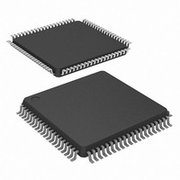
Package / Case
80-LQFP
Lead Free Status / RoHS Status
Lead free / RoHS Compliant
Eeprom Size
-
Lead Free Status / RoHS Status
Lead free / RoHS Compliant
Available stocks
Company
Part Number
Manufacturer
Quantity
Price
Company:

Part Number:
ADUC7126BSTZ126-RL
Manufacturer:
Analog Devices Inc
Quantity:
10 000


ADuC7124/ADuC7126
COM1CON0 Register
Name:
Address:
Default Value:
Access:
COM1CON0 is the line control register for UART1.
Table 95. COMxCON0 MMR Bit Descriptions
Bit
7
6
5
4
3
2
[1:0]
COM0CON1 Register
Name:
Address:
Default Value:
Access:
COM0CON1 is the modem control register for UART0.
Name
DLAB
BRK
SP
EPS
PEN
Stop
WLS
Description
Divisor latch access.
Set by the user to enable access to the
COMxDIV0 and COMxDIV1 registers.
Cleared by the user to disable access to
COMxDIV0 and COMxDIV1 and enable access to
COMxRX and COMxTX.
Set break.
Set by the user to force SOUTx to 0.
Cleared to operate in normal mode.
Stick parity.
Set by the user to force parity to defined values:
1 if EPS = 1 and PEN = 1, 0 if EPS = 0 and PEN = 1.
Even parity select bit.
Set for even parity.
Cleared for odd parity.
Parity enable bit.
Set by the user to transmit and check the
parity bit.
Cleared by the user for no parity transmission or
checking.
Stop bit.
Set by the user to transmit 1½ stop bits if the word
length is five bits or two stop bits if the word
length is six bits, seven bits, or eight bits. The
receiver checks the first stop bit only, regardless
of the number of stop bits selected.
Cleared by the user to generate one stop bit in
the transmitted data.
Word length select:
00 = five bits, 01 = six bits, 10 = seven bits, 11 =
eight bits.
COM1CON0
0xFFFF074C
COM0CON1
0xFFFF0710
0x00
Read/write
0x00
Read/write
Rev. B | Page 64 of 104
COM1CON1 Register
Name:
Address:
Default Value:
Access:
COM1CON1 is the modem control register for UART1.
Table 96. COMxCON1 MMR Bit Descriptions
Bit
[7:5]
4
3
2
1
0
COM0STA0 Register
Name:
Address:
Default Value:
Access:
COM0STA0 is the line status register for UART0.
Name
LOOPBACK
PEN
Stop
RTS
DTR
Description
Reserved.
Loop back.
Set by the user to enable loopback mode.
In loopback mode, SOUTx is forced high.
The modem signals are also directly con-
nected to the status inputs (RTS to CTS and
DTR to DSR).
Cleared by the user to be in normal mode.
Parity enable bit.
Set by the user to transmit and check the
parity bit.
Cleared by the user for no parity transmission
or checking.
Stop bit.
Set by the user to transmit 1½ stop bits if
the word length is five bits or two stop bits
if the word length is six bits, seven bits, or
eight bits. The receiver checks the first stop
bit only, regardless of the number of stop
bits selected.
Cleared by the user to generate one stop
bit in the transmitted data.
Request to send.
Set by the user to force the RTS output to 0.
Cleared by the user to force the RTS output
to 1.
Data terminal ready.
Set by the user to force the DTR output to
0.
Cleared by the user to force the DTR output
to 1.
COM1CON1
0xFFFF0750
0x00
Read/write
COM0STA0
0xFFFF0714
0xE0
Read only
Related parts for ADUC7126BSTZ126-RL
Image
Part Number
Description
Manufacturer
Datasheet
Request
R

Part Number:
Description:
Precision Analog Microcontroller, 12-Bit Analog I/O, Large Memory, ARM7TDMI MCU with Enhanced IRQ Handler
Manufacturer:
Analog Devices
Datasheet:

Part Number:
Description:
±1.7g Dual-Axis IMEMS Accelerometer Evaluation Board
Manufacturer:
Analog Devices Inc
Datasheet:

Part Number:
Description:
Inertial Sensor Evaluation System
Manufacturer:
Analog Devices Inc
Datasheet:
Part Number:
Description:
Manufacturer:
Analog Devices Inc
Datasheet:
Part Number:
Description:
Manufacturer:
Analog Devices Inc
Datasheet:
Part Number:
Description:
Manufacturer:
Analog Devices Inc
Datasheet:
Part Number:
Description:
Manufacturer:
Analog Devices Inc
Datasheet:
Part Number:
Description:
Manufacturer:
Analog Devices Inc
Datasheet:
Part Number:
Description:
Manufacturer:
Analog Devices Inc
Datasheet:
Part Number:
Description:
Manufacturer:
Analog Devices Inc
Datasheet:
Part Number:
Description:
Manufacturer:
Analog Devices Inc
Datasheet:
Part Number:
Description:
Manufacturer:
Analog Devices Inc
Datasheet:
Part Number:
Description:
Manufacturer:
Analog Devices Inc
Datasheet: