ADUC7126BSTZ126-RL Analog Devices Inc, ADUC7126BSTZ126-RL Datasheet - Page 69
ADUC7126BSTZ126-RL
Manufacturer Part Number
ADUC7126BSTZ126-RL
Description
ARM7 With 12-Bit ADC & DACs, 128kB Flash
Manufacturer
Analog Devices Inc
Series
MicroConverter® ADuC7xxxr
Datasheet
1.ADUC7126BSTZ126.pdf
(104 pages)
Specifications of ADUC7126BSTZ126-RL
Core Processor
ARM7
Core Size
16/32-Bit
Speed
41.78MHz
Connectivity
EBI/EMI, I²C, SPI, UART/USART
Peripherals
POR, PWM, WDT
Number Of I /o
40
Program Memory Size
126KB (126K x 8)
Program Memory Type
FLASH
Ram Size
32K x 8
Voltage - Supply (vcc/vdd)
2.7 V ~ 3.6 V
Data Converters
A/D 12x12b, D/A 4x12b
Oscillator Type
Internal
Operating Temperature
-40°C ~ 125°C
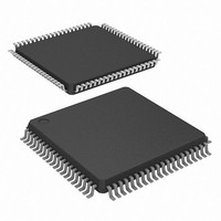
Package / Case
80-LQFP
Lead Free Status / RoHS Status
Lead free / RoHS Compliant
Eeprom Size
-
Lead Free Status / RoHS Status
Lead free / RoHS Compliant
Available stocks
Company
Part Number
Manufacturer
Quantity
Price
Company:

Part Number:
ADUC7126BSTZ126-RL
Manufacturer:
Analog Devices Inc
Quantity:
10 000


Bit
9
8
7
6
5
4
3
2
1
0
Name
SPIOEN
SPIROW
SPIZEN
SPITMDE
SPILF
SPIWOM
SPICPO
SPICPH
SPIMEN
SPIEN
Description
Slave MISO output enable bit.
Set this bit for MISO to operate as normal.
Clear this bit to disable the output driver on the MISO pin. The MISO pin is open-drain when this bit is cleared.
SPIRX overflow overwrite enable.
Set by the user, the valid data in the SPIRX register is overwritten by the new serial byte received.
Cleared by the user, the new serial byte received is discarded.
SPI transmits zeros when Tx FIFO is empty.
Set this bit to transmit 0x00 when there is no valid data in the Tx FIFO.
Clear this bit to transmit the last transmitted value when there is no valid data in the Tx FIFO.
SPI transfer and interrupt mode.
Set by the user to initiate transfer with a write to the SPITX register. Interrupt occurs only when SPITX is empty.
Cleared by the user to initiate transfer with a read of the SPIRX register. Interrupt occurs only when SPIRX is full.
LSB first transfer enable bit.
Set by the user, the LSB is transmitted first.
Cleared by the user, the MSB is transmitted first.
SPI wire-OR’ed mode enable bit.
Set to 1 enable open-drain data output. External pull-ups required on data output pins.
Cleared for normal output levels.
Serial clock polarity mode bit.
Set by the user, the serial clock idles high.
Cleared by the user, the serial clock idles low.
Serial clock phase mode bit.
Set by the user, the serial clock pulses at the beginning of each serial bit transfer.
Cleared by the user, the serial clock pulses at the end of each serial bit transfer.
Master mode enable bit.
Set by the user to enable master mode.
Cleared by the user to enable slave mode.
SPI enable bit.
Set by the user to enable the SPI.
Cleared by the user to disable the SPI.
Rev. B | Page 69 of 104
ADuC7124/ADuC7126
Related parts for ADUC7126BSTZ126-RL
Image
Part Number
Description
Manufacturer
Datasheet
Request
R

Part Number:
Description:
Precision Analog Microcontroller, 12-Bit Analog I/O, Large Memory, ARM7TDMI MCU with Enhanced IRQ Handler
Manufacturer:
Analog Devices
Datasheet:

Part Number:
Description:
±1.7g Dual-Axis IMEMS Accelerometer Evaluation Board
Manufacturer:
Analog Devices Inc
Datasheet:

Part Number:
Description:
Inertial Sensor Evaluation System
Manufacturer:
Analog Devices Inc
Datasheet:
Part Number:
Description:
Manufacturer:
Analog Devices Inc
Datasheet:
Part Number:
Description:
Manufacturer:
Analog Devices Inc
Datasheet:
Part Number:
Description:
Manufacturer:
Analog Devices Inc
Datasheet:
Part Number:
Description:
Manufacturer:
Analog Devices Inc
Datasheet:
Part Number:
Description:
Manufacturer:
Analog Devices Inc
Datasheet:
Part Number:
Description:
Manufacturer:
Analog Devices Inc
Datasheet:
Part Number:
Description:
Manufacturer:
Analog Devices Inc
Datasheet:
Part Number:
Description:
Manufacturer:
Analog Devices Inc
Datasheet:
Part Number:
Description:
Manufacturer:
Analog Devices Inc
Datasheet:
Part Number:
Description:
Manufacturer:
Analog Devices Inc
Datasheet: