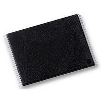
NAND01GW3B2BN6E NUMONYX, NAND01GW3B2BN6E Datasheet - Page 45

NAND01GW3B2BN6E
Manufacturer Part Number
NAND01GW3B2BN6E
Description
IC, FLASH, 1GB, 25µS, TSOP-48
Manufacturer
NUMONYX
Specifications of NAND01GW3B2BN6E
Memory Type
Flash
Memory Size
1GB
Access Time
25µs
Supply Voltage Range
2.7V To 3.6V
Memory Case Style
TSOP
No. Of Pins
48
Operating Temperature Range
-40°C To +85°C
Voltage, Vcc
3.3V
Rohs Compliant
Yes
Interface
Serial
Lead Free Status / RoHS Status
Lead free / RoHS Compliant
Available stocks
Company
Part Number
Manufacturer
Quantity
Price
Part Number:
NAND01GW3B2BN6E
Manufacturer:
ST
Quantity:
20 000
NAND01G-B2B, NAND02G-B2C
Table 25.
1. The time to ready depends on the value of the pull-up resistor tied to the ready/busy pin. See
2.
3. During a program/erase enable operation, t
4. ES = electronic signature.
Symbol
t
t
t
t
t
t
t
t
t
t
t
ALLRL1
ALLRL2
t
t
t
t
t
t
t
t
t
WHWH
t
t
t
t
BLBH1
BLBH2
BLBH3
BLBH4
BLBH5
t
CLLRL
VHWH
WHBH
EHQX
RHQX
WHBL
WHRL
EHQZ
RHQZ
VLWH
RHRL
RLRH
RLQV
BHRL
DZRL
ELQV
RLRL
Figure
During a program/erase disable Operation, t
t
WHWH
33.
is the time from W rising edge during the final address cycle to W rising edge during the first data cycle.
symbol
t
t
t
t
t
ADL
t
PROG
t
t
WW
t
t
t
BERS
t
CBSY
t
T
Alt.
t
WHR
AC characteristics for operations
t
t
RST
CLR
CHZ
RHZ
CEA
REH
t
t
REA
t
WB
RR
RC
t
AR
RP
IR
OH
R
(2)
(3)
Address Latch Low to
Read Enable Low
Ready/Busy High to Read Enable Low
Ready/Busy Low to
Ready/Busy High
Command Latch Low to Read Enable Low
Data Hi-Z to Read Enable Low
Chip Enable High to Output Hi-Z
Last address latched to data loading time during program
operations
Write protection time
Chip Enable Low to Output Valid
Read Enable High to
Read Enable Low
Chip Enable High or Read Enable high to Output Hold
Read Enable Low to
Read Enable High
Read Enable Low to
Read Enable Low
Read Enable Low to
Output Valid
Write Enable High to
Ready/Busy High
Write Enable High to Ready/Busy Low
Write Enable High to Read Enable Low
Read Enable High to Output Hi-z
WW
WW
Read electronic signature
Read cycle
Read busy time
Program busy time
Erase busy time
Reset busy time, during ready
Reset busy time, during read
Reset busy time, during program
Reset busy time, during erase
Cache busy time
Read Enable High hold time
Read Enable pulse width
Read cycle time
Read Enable access time
Read ES access time
Read busy time
is the delay from WP high to W High.
is the delay from WP Low to W High.
Parameter
(1)
(4)
Max
Max
Max
Max
Max
Max
Max
Max
Max
Max
Max
Max
Max
Max
Min
Min
Min
Typ
Min
Min
Min
Min
Min
Min
Min
Min
Min
Figure
DC and AC parameters
devices
1.8 V
700
500
700
100
100
100
10
10
20
25
10
10
30
30
45
15
10
25
50
30
25
60
3
5
5
3
0
31,
Figure 32
devices
700
500
700
100
100
100
3 V
10
10
20
25
10
10
30
30
25
10
10
15
30
20
25
60
3
5
5
3
0
and
45/60
Unit
ms
ns
ns
ns
µs
µs
µs
µs
µs
µs
µs
µs
ns
ns
ns
ns
ns
ns
ns
ns
ns
ns
ns
ns
µs
ns
ns


