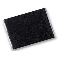
NAND01GW3B2BN6E NUMONYX, NAND01GW3B2BN6E Datasheet - Page 31

NAND01GW3B2BN6E
Manufacturer Part Number
NAND01GW3B2BN6E
Description
IC, FLASH, 1GB, 25µS, TSOP-48
Manufacturer
NUMONYX
Specifications of NAND01GW3B2BN6E
Memory Type
Flash
Memory Size
1GB
Access Time
25µs
Supply Voltage Range
2.7V To 3.6V
Memory Case Style
TSOP
No. Of Pins
48
Operating Temperature Range
-40°C To +85°C
Voltage, Vcc
3.3V
Rohs Compliant
Yes
Interface
Serial
Lead Free Status / RoHS Status
Lead free / RoHS Compliant
Available stocks
Company
Part Number
Manufacturer
Quantity
Price
Part Number:
NAND01GW3B2BN6E
Manufacturer:
ST
Quantity:
20 000
NAND01G-B2B, NAND02G-B2C
6.8.4
6.8.5
6.8.6
Table 13.
1. Only valid for cache program operations, for other operations it is same as SR6.
2. Only valid for cache operations, for other operations it is don’t care.
SR4, SR3, SR2
SR7
SR6
SR5
SR1
SR0
Bit
Cache program error bit (SR1)
The cache program error bit can be used to identify if the previous page (page N-1) has been
successfully programmed or not in a cache program operation. SR1 is set to ’1’ when the
cache program operation has failed to program the previous page (page N-1) correctly. If
SR1 is set to ‘0’ the operation has completed successfully.
The cache program error bit is only valid during cache program operations, during other
operations it is don’t care.
Error bit (SR0)
The error bit is used to identify if any errors have been detected by the P/E/R controller. The
error bit is set to ’1’ when a program or erase operation has failed to write the correct data to
the memory. If the error bit is set to ‘0’ the operation has completed successfully. The error
bit SR0, in a cache program operation, indicates a failure on page N.
SR4, SR3 and SR2 are reserved
Status register bits
Cache program error
Program/ erase/ read
Program/ erase/ read
Cache program error
Cache ready/busy
Write protection
Generic error
controller
Reserved
controller
Name
(1)
(2)
Logic level
Don’t care
‘1’
‘0’
‘1’
‘0’
'1'
'0'
'1'
'0'
'1'
'0'
'1'
'0'
'1'
'0'
Not protected
Protected
P/E/R C inactive, device ready
P/E/R C active, device busy
Cache register ready (cache operation only)
Cache register busy (cache operation only)
P/E/R C inactive, device ready
P/E/R C active, device busy
Page N-1 failed in cache program operation
Page N-1 programmed successfully
Error – operation failed
No Error – operation successful
Page N failed in cache program operation
Page N programmed successfully
Definition
Device operations
31/60


