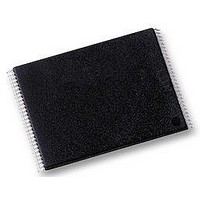
NAND01GW3B2BN6E NUMONYX, NAND01GW3B2BN6E Datasheet - Page 35

NAND01GW3B2BN6E
Manufacturer Part Number
NAND01GW3B2BN6E
Description
IC, FLASH, 1GB, 25µS, TSOP-48
Manufacturer
NUMONYX
Specifications of NAND01GW3B2BN6E
Memory Type
Flash
Memory Size
1GB
Access Time
25µs
Supply Voltage Range
2.7V To 3.6V
Memory Case Style
TSOP
No. Of Pins
48
Operating Temperature Range
-40°C To +85°C
Voltage, Vcc
3.3V
Rohs Compliant
Yes
Interface
Serial
Lead Free Status / RoHS Status
Lead free / RoHS Compliant
Available stocks
Company
Part Number
Manufacturer
Quantity
Price
Part Number:
NAND01GW3B2BN6E
Manufacturer:
ST
Quantity:
20 000
NAND01G-B2B, NAND02G-B2C
8
8.1
8.2
Software algorithms
This section gives information on the software algorithms that Numonyx recommends to
implement to manage the bad blocks and extend the lifetime of the NAND device.
NAND flash memories are programmed and erased by Fowler-Nordheim tunneling using a
high voltage. Exposing the device to a high voltage for extended periods can cause the
oxide layer to be damaged. For this reason, the number of program and erase cycles is
limited (see
wear-leveling algorithm and an error correction code, to extend the number of program and
erase cycles and increase the data retention.
To help integrate a NAND memory into an application, Numonyx can provide a file system
OS native reference software, which supports the basic commands of file management.
Contact the nearest Numonyx sales office for more details.
Bad block management
Devices with bad blocks have the same quality level and the same AC and DC
characteristics as devices where all the blocks are valid. A bad block does not affect the
performance of valid blocks because it is isolated from the bit line and common source line
by a select transistor.
The devices are supplied with all the locations inside valid blocks erased (FFh). The bad
block information is written prior to shipping. Any block, where the 1st and 6th bytes, or 1st
word, in the spare area of the 1st page, does not contain FFh, is a bad block.
The bad block Information must be read before any erase is attempted as the bad block
information may be erased. For the system to be able to recognize the bad blocks based on
the original information it is recommended to create a bad block table following the flowchart
shown in
NAND flash memory failure modes
Over the lifetime of the device additional bad blocks may develop.
To implement a highly reliable system, all the possible failure modes must be considered:
Refer to
Program/erase failure: in this case the block has to be replaced by copying the data to
a valid block. These additional bad blocks can be identified as attempts to program or
erase them will give errors in the status register
As the failure of a page program operation does not affect the data in other pages in the
same block, the block can be replaced by re-programming the current data and copying
the rest of the replaced block to an available valid block. The Copy Back Program
command can be used to copy the data to a valid block. See
program
Read failure: in this case, ECC correction must be implemented. To efficiently use the
memory space, it is recommended to recover single-bit error in read by ECC, without
replacing the whole block.
Table 17
Figure
Table 18
for more details
15.
for the procedure to follow if an error occurs during an operation.
for value) and it is recommended to implement garbage collection, a
Section 6.4: Copy back
Software algorithms
35/60


