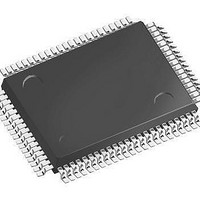
SAF-XC164CS-32F40F BB-A Infineon Technologies, SAF-XC164CS-32F40F BB-A Datasheet - Page 34

SAF-XC164CS-32F40F BB-A
Manufacturer Part Number
SAF-XC164CS-32F40F BB-A
Description
IC MCU 16BIT 256KB FLSH 100TQFP
Manufacturer
Infineon Technologies
Series
XC16xr
Datasheet
1.SAK-XC164CS-32F20F_BB-A.pdf
(81 pages)
Specifications of SAF-XC164CS-32F40F BB-A
Core Processor
C166SV2
Core Size
16-Bit
Speed
40MHz
Connectivity
CAN, EBI/EMI, SPI, UART/USART
Peripherals
PWM, WDT
Number Of I /o
79
Program Memory Size
256KB (256K x 8)
Program Memory Type
FLASH
Ram Size
12K x 8
Voltage - Supply (vcc/vdd)
2.35 V ~ 2.7 V
Data Converters
A/D 14x8/10b
Oscillator Type
Internal
Operating Temperature
-40°C ~ 85°C
Package / Case
100-LFQFP
Data Bus Width
16 bit
Data Ram Size
12 KB
Interface Type
2xASC, 2xSSC
Maximum Clock Frequency
40 MHz
Number Of Programmable I/os
79
Number Of Timers
11
Operating Supply Voltage
5 V
Maximum Operating Temperature
+ 85 C
Mounting Style
SMD/SMT
Minimum Operating Temperature
- 40 C
On-chip Adc
10 bit, 14 Channel
Packages
PG-TQFP-100
Max Clock Frequency
40.0 MHz
Sram (incl. Cache)
12.0 KByte
Can Nodes
2
A / D Input Lines (incl. Fadc)
14
Program Memory
256.0 KByte
Lead Free Status / RoHS Status
Lead free / RoHS Compliant
Eeprom Size
-
Lead Free Status / Rohs Status
Details
3.7
The CAPCOM6 unit supports generation and control of timing sequences on up to three
16-bit capture/compare channels plus one independent 10-bit compare channel.
In compare mode the CAPCOM6 unit provides two output signals per channel which
have inverted polarity and non-overlapping pulse transitions (deadtime control). The
compare channel can generate a single PWM output signal and is further used to
modulate the capture/compare output signals.
In capture mode the contents of compare timer T12 is stored in the capture registers
upon a signal transition at pins CCx.
Compare timers T12 (16-bit) and T13 (10-bit) are free running timers which are clocked
by the prescaled system clock.
Figure 6
For motor control applications both subunits may generate versatile multichannel PWM
signals which are basically either controlled by compare timer T12 or by a typical hall
sensor pattern at the interrupt inputs (block commutation).
Data Sheet
f
f
CPU
CPU
The timer registers (T12, T13) are not directly accessible.
The period and offset registers are loading a value into the timer registers.
The Capture/Compare Unit CAPCOM6
CAPCOM6 Block Diagram
Period Register
Period Register
Control Register
Offset Register
Timer T12
Timer T13
Compare
Compare
T12P
T13P
CTCON
T12OF
16-bit
10-bit
Select Register
Compare Register
CC6MSEL
CC Channel 0
CC Channel 1
CC Channel 2
Mode
CMP13
CC60
CC61
CC62
32
Trap Register
CC6MCON.H
Commutation
Control
Control
Block
Logic
Port
Functional Description
CC6POS0
CC6POS1
CC6POS2
CTRAP
CC60
COUT60
CC61
COUT61
CC62
COUT62
COUT63
Derivatives
V1.1, 2006-08
MCB04109
XC164-32


