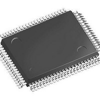
SAF-XC164CS-32F40F BB-A Infineon Technologies, SAF-XC164CS-32F40F BB-A Datasheet - Page 22

SAF-XC164CS-32F40F BB-A
Manufacturer Part Number
SAF-XC164CS-32F40F BB-A
Description
IC MCU 16BIT 256KB FLSH 100TQFP
Manufacturer
Infineon Technologies
Series
XC16xr
Datasheet
1.SAK-XC164CS-32F20F_BB-A.pdf
(81 pages)
Specifications of SAF-XC164CS-32F40F BB-A
Core Processor
C166SV2
Core Size
16-Bit
Speed
40MHz
Connectivity
CAN, EBI/EMI, SPI, UART/USART
Peripherals
PWM, WDT
Number Of I /o
79
Program Memory Size
256KB (256K x 8)
Program Memory Type
FLASH
Ram Size
12K x 8
Voltage - Supply (vcc/vdd)
2.35 V ~ 2.7 V
Data Converters
A/D 14x8/10b
Oscillator Type
Internal
Operating Temperature
-40°C ~ 85°C
Package / Case
100-LFQFP
Data Bus Width
16 bit
Data Ram Size
12 KB
Interface Type
2xASC, 2xSSC
Maximum Clock Frequency
40 MHz
Number Of Programmable I/os
79
Number Of Timers
11
Operating Supply Voltage
5 V
Maximum Operating Temperature
+ 85 C
Mounting Style
SMD/SMT
Minimum Operating Temperature
- 40 C
On-chip Adc
10 bit, 14 Channel
Packages
PG-TQFP-100
Max Clock Frequency
40.0 MHz
Sram (incl. Cache)
12.0 KByte
Can Nodes
2
A / D Input Lines (incl. Fadc)
14
Program Memory
256.0 KByte
Lead Free Status / RoHS Status
Lead free / RoHS Compliant
Eeprom Size
-
Lead Free Status / Rohs Status
Details
5) Several pipeline optimizations are not active within the external IO area. This is necessary to control external
3.2
All of the external memory accesses are performed by a particular on-chip External Bus
Controller (EBC). It can be programmed either to Single Chip Mode when no external
memory is required, or to one of four different external memory access modes
are as follows:
•
•
•
•
In the demultiplexed bus modes, addresses are output on PORT1 and data is
input/output on PORT0 or P0L, respectively. In the multiplexed bus modes both
addresses and data use PORT0 for input/output. The high order address (segment) lines
use Port 4. The number of active segment address lines is selectable, restricting the
external address space to 8 Mbytes … 64 Kbytes. This is required when interface lines
are assigned to Port 4.
Up to 4 external CS signals (3 windows plus default) can be generated in order to save
external glue logic. External modules can directly be connected to the common
address/data bus and their individual select lines.
Important timing characteristics of the external bus interface have been made
programmable (via registers TCONCSx/FCONCSx) to allow the user the adaption of a
wide range of different types of memories and external peripherals.
In addition, up to 4 independent address windows may be defined (via registers
ADDRSELx) which control the access to different resources with different bus
characteristics. These address windows are arranged hierarchically where window 4
overrides window 3, and window 2 overrides window 1. All accesses to locations not
covered by these 4 address windows are controlled by TCONCS0/FCONCS0. The
currently active window can generate a chip select signal.
Note: The chip select signal of address window 4 is not available on a pin.
The external bus timing is related to the rising edge of the reference clock output
CLKOUT. The external bus protocol is compatible with that of the standard C166 Family.
The EBC also controls accesses to resources connected to the on-chip LXBus. The
LXBus is an internal representation of the external bus and allows accessing integrated
peripherals and modules in the same way as external components.
The TwinCAN module is connected and accessed via the LXBus.
1) Bus modes are switched dynamically if several address windows with different mode settings are used.
Data Sheet
peripherals properly.
16 … 24-bit Addresses, 16-bit Data, Demultiplexed
16 … 24-bit Addresses, 16-bit Data, Multiplexed
16 … 24-bit Addresses, 8-bit Data, Multiplexed
16 … 24-bit Addresses, 8-bit Data, Demultiplexed
External Bus Controller
20
Functional Description
Derivatives
V1.1, 2006-08
XC164-32
1)
, which


