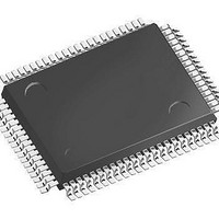
SAF-XC164CS-32F40F BB-A Infineon Technologies, SAF-XC164CS-32F40F BB-A Datasheet - Page 21

SAF-XC164CS-32F40F BB-A
Manufacturer Part Number
SAF-XC164CS-32F40F BB-A
Description
IC MCU 16BIT 256KB FLSH 100TQFP
Manufacturer
Infineon Technologies
Series
XC16xr
Datasheet
1.SAK-XC164CS-32F20F_BB-A.pdf
(81 pages)
Specifications of SAF-XC164CS-32F40F BB-A
Core Processor
C166SV2
Core Size
16-Bit
Speed
40MHz
Connectivity
CAN, EBI/EMI, SPI, UART/USART
Peripherals
PWM, WDT
Number Of I /o
79
Program Memory Size
256KB (256K x 8)
Program Memory Type
FLASH
Ram Size
12K x 8
Voltage - Supply (vcc/vdd)
2.35 V ~ 2.7 V
Data Converters
A/D 14x8/10b
Oscillator Type
Internal
Operating Temperature
-40°C ~ 85°C
Package / Case
100-LFQFP
Data Bus Width
16 bit
Data Ram Size
12 KB
Interface Type
2xASC, 2xSSC
Maximum Clock Frequency
40 MHz
Number Of Programmable I/os
79
Number Of Timers
11
Operating Supply Voltage
5 V
Maximum Operating Temperature
+ 85 C
Mounting Style
SMD/SMT
Minimum Operating Temperature
- 40 C
On-chip Adc
10 bit, 14 Channel
Packages
PG-TQFP-100
Max Clock Frequency
40.0 MHz
Sram (incl. Cache)
12.0 KByte
Can Nodes
2
A / D Input Lines (incl. Fadc)
14
Program Memory
256.0 KByte
Lead Free Status / RoHS Status
Lead free / RoHS Compliant
Eeprom Size
-
Lead Free Status / Rohs Status
Details
RH7) so-called General Purpose Registers (GPRs).
The upper 256 bytes of the DPRAM are directly bitaddressable. When used by a GPR,
any location in the DPRAM is bitaddressable.
1024 bytes (2 × 512 bytes) of the address space are reserved for the Special Function
Register areas (SFR space and ESFR space). SFRs are wordwide registers which are
used for controlling and monitoring functions of the different on-chip units. Unused SFR
addresses are reserved for future members of the XC166 Family. Therefore, they should
either not be accessed, or written with zeros, to ensure upward compatibility.
In order to meet the needs of designs where more memory is required than is provided
on chip, up to 12 Mbytes (approximately, see
be connected to the microcontroller. The External Bus Interface also provides access to
external peripherals.
Table 3
Address Area
Flash register space
Reserved (Acc. trap)
Reserved for EPSRAM F8’1800
Emul. Program
SRAM
Reserved for PSRAM
Program SRAM
Reserved for program
memory
Program Flash/ROM
Reserved
External memory area 40’0000
External IO area
TwinCAN registers
External memory area 01’0000
Data RAMs and SFRs 00’8000
External memory area 00’0000
1) Accesses to the shaded areas generate external bus accesses.
2) The areas marked with “<” are slightly smaller than indicated, see column “Notes”.
3) Not defined register locations return a trap code.
4) The Emulation PSRAM (EPSRAM) realizes a 2
Data Sheet
4)
XC164CS Memory Map
5)
Start Loc.
FF’F000
FE’0000
F8’0000
E0’1800
E0’0000
C4’0000
C0’0000
BF’0000
20’0800
20’0000
H
H
H
H
H
H
H
H
H
H
H
H
H
H
H
End Loc.
FF’FFFF
FF’EFFF
FD’FFFF
F8’17FF
F7’FFFF
E0’17FF
DF’FFFF
C3’FFFF
BF’FFFF
BE’FFFF
3F’FFFF
20’07FF
1F’FFFF
00’FFFF
00’7FFF
1)
nd
access path to the PSRAM with a different timing.
19
Table
H
H
H
H
H
H
H
H
H
H
H
H
H
H
H
Area Size
4 Kbytes
60 Kbytes
378 Kbytes
6 Kbytes
< 1.5 Mbytes Minus PSRAM
6 Kbytes
< 2 Mbytes
256 Kbytes
64 Kbytes
< 8 Mbytes
< 2 Mbytes
2 Kbytes
< 2 Mbytes
32 Kbytes
32 Kbytes
3) of external RAM and/or ROM can
2)
Functional Description
Notes
3)
–
–
2
Maximum
Minus Flash
–
–
Minus reserved
segment
Minus TwinCAN
–
Minus segment 0
Partly used
–
nd
way to PSRAM
Derivatives
V1.1, 2006-08
XC164-32


