M30835FJGP#U5 Renesas Electronics America, M30835FJGP#U5 Datasheet - Page 88
M30835FJGP#U5
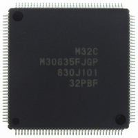
Manufacturer Part Number
M30835FJGP#U5
Description
IC M32C/83 MCU FLASH 144LQFP
Manufacturer
Renesas Electronics America
Series
M16C™ M32C/80r
Datasheets
1.M3087BFLGPU3.pdf
(364 pages)
2.M30833FJGPU3.pdf
(96 pages)
3.M30833FJGPU3.pdf
(529 pages)
Specifications of M30835FJGP#U5
Core Processor
M32C/80
Core Size
16/32-Bit
Speed
32MHz
Connectivity
CAN, I²C, IEBus, SIO, UART/USART
Peripherals
DMA, WDT
Number Of I /o
121
Program Memory Size
512KB (512K x 8)
Program Memory Type
FLASH
Ram Size
31K x 8
Voltage - Supply (vcc/vdd)
3 V ~ 5.5 V
Data Converters
A/D 34x10b, D/A 2x8b
Oscillator Type
Internal
Operating Temperature
-20°C ~ 85°C
Package / Case
144-LQFP
For Use With
R0K330879S001BE - KIT DEV RSK M32C/87R0K330879S000BE - KIT DEV RSK M32C/87
Lead Free Status / RoHS Status
Lead free / RoHS Compliant
Eeprom Size
-
Available stocks
Company
Part Number
Manufacturer
Quantity
Price

Part Number:
M30835FJGP#U5M30835FJGP#U3
Manufacturer:
Renesas Electronics America
Quantity:
10 000


R
R
M
e
E
. v
J
3
Figure 7.7 RD Signal Output Extended by RDY Signal
Figure 7.8 Order of Bus Priority
0
2
7.2.7 HOLD Signal
1
9
C
3 .
B
The HOLD signal transfers bus privileges from the CPU to external circuits. When an "L" signal is applied
to the HOLD pin , the microcomputer enters a hold state after bus access is completed. While the HOLD
pin is held "L", the microcomputer is in a hold state and the HLDA pin outputs an "L" signal. Table 7.7
shows the microcomputer status in a hold state.
Bus is used in the following order of priority: HOLD, DMAC, CPU.
8 /
0
1
0
3
3
J
__________
G
4
a
0 -
n
_________
__________
o r
3 .
1
u
, 1
3
(2) Multiplexed Bus with 2 Wait States
(1) Separate Bus with 2 Wait States
_____
p
1
2
NOTES:
(
0
M
BCLK
RD
CS
(i=0 to 3)
RDY
BCLK
RD
CS
(i=0 to 3)
RDY
1. The chip-select signal (CSi) may be extended depending on CPU state such as the instruction
0
3
6
tsu
Timing to receive RDY for j wait(s): j+1 cycles (j = 1 to 3)
i
i
queue buffer.
2
(1)
(1)
C
(RDY-BCLK)
8 /
: Wait states inserted by RDY
: Wait states inserted by program
Page 63
, 3
M
3
1st cycle
1st cycle
: Setup time for RDY input
2
C
f o
8 /
4
8
3
8
) T
__________
HOLD > DMAC > CPU
2nd cycle
2nd cycle
________
__________
Timing to receive RDY
Timing to receive RDY
3rd cycle
3rd cycle
tsu(RDY - BCLK)
tsu(RDY - BCLK)
_________
4th cycle
4th cycle
__________
7. Bus
Related parts for M30835FJGP#U5
Image
Part Number
Description
Manufacturer
Datasheet
Request
R

Part Number:
Description:
KIT STARTER FOR M16C/29
Manufacturer:
Renesas Electronics America
Datasheet:

Part Number:
Description:
KIT STARTER FOR R8C/2D
Manufacturer:
Renesas Electronics America
Datasheet:

Part Number:
Description:
R0K33062P STARTER KIT
Manufacturer:
Renesas Electronics America
Datasheet:

Part Number:
Description:
KIT STARTER FOR R8C/23 E8A
Manufacturer:
Renesas Electronics America
Datasheet:

Part Number:
Description:
KIT STARTER FOR R8C/25
Manufacturer:
Renesas Electronics America
Datasheet:

Part Number:
Description:
KIT STARTER H8S2456 SHARPE DSPLY
Manufacturer:
Renesas Electronics America
Datasheet:

Part Number:
Description:
KIT STARTER FOR R8C38C
Manufacturer:
Renesas Electronics America
Datasheet:

Part Number:
Description:
KIT STARTER FOR R8C35C
Manufacturer:
Renesas Electronics America
Datasheet:

Part Number:
Description:
KIT STARTER FOR R8CL3AC+LCD APPS
Manufacturer:
Renesas Electronics America
Datasheet:
Part Number:
Description:
KIT STARTER FOR RX610
Manufacturer:
Renesas Electronics America
Datasheet:

Part Number:
Description:
KIT STARTER FOR R32C/118
Manufacturer:
Renesas Electronics America
Datasheet:

Part Number:
Description:
KIT DEV RSK-R8C/26-29
Manufacturer:
Renesas Electronics America
Datasheet:

Part Number:
Description:
KIT STARTER FOR SH7124
Manufacturer:
Renesas Electronics America
Datasheet:

Part Number:
Description:
KIT STARTER FOR H8SX/1622
Manufacturer:
Renesas Electronics America
Datasheet:

Part Number:
Description:
KIT DEV FOR SH7203
Manufacturer:
Renesas Electronics America
Datasheet: