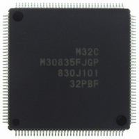
M30835FJGP#U5 Renesas Electronics America, M30835FJGP#U5 Datasheet - Page 524

M30835FJGP#U5
Manufacturer Part Number
M30835FJGP#U5
Description
IC M32C/83 MCU FLASH 144LQFP
Manufacturer
Renesas Electronics America
Series
M16C™ M32C/80r
Datasheets
1.M3087BFLGPU3.pdf
(364 pages)
2.M30833FJGPU3.pdf
(96 pages)
3.M30833FJGPU3.pdf
(529 pages)
Specifications of M30835FJGP#U5
Core Processor
M32C/80
Core Size
16/32-Bit
Speed
32MHz
Connectivity
CAN, I²C, IEBus, SIO, UART/USART
Peripherals
DMA, WDT
Number Of I /o
121
Program Memory Size
512KB (512K x 8)
Program Memory Type
FLASH
Ram Size
31K x 8
Voltage - Supply (vcc/vdd)
3 V ~ 5.5 V
Data Converters
A/D 34x10b, D/A 2x8b
Oscillator Type
Internal
Operating Temperature
-20°C ~ 85°C
Package / Case
144-LQFP
For Use With
R0K330879S001BE - KIT DEV RSK M32C/87R0K330879S000BE - KIT DEV RSK M32C/87
Lead Free Status / RoHS Status
Lead free / RoHS Compliant
Eeprom Size
-
Available stocks
Company
Part Number
Manufacturer
Quantity
Price
Part Number:
M30835FJGP#U5M30835FJGP#U3
Manufacturer:
Renesas Electronics America
Quantity:
10 000
- Current page: 524 of 529
- Download datasheet (5Mb)
Rev.
1.31
1.20
REVISION HISTORY
2006-1
2004-6
Date
450 to 472 • Overall structure modified
All Pages
All pages Words standardized: On-chip oscillator, A/D converter and D/A converter
416, 434 • Tables 26.6 Flash Memory Version Electrical Characteristics added
All Pages Word standardized: Clock Generation Circuit , On-chip Oscillator, A/D Converter,
22 to 23
Page
413
414
416
111
112
432
449
2, 3
21
45
1
5
Electrical Characteristics
• Table 26.1 Absolute Maximum Ratings V
• Table 26.2 Recommended Operation Conditions (V
• Table 26.4 A/D Conversion Characteristics
Precautions
Interrupts
• Figure 10.15 IIO0IE to IIO11IE Registers Note 2 added
Watchdog Timer
• Figure 11.1 Watchdog Timer Block Diagram modified
Electrical Characteristics
• Figure 26.8 V
• Figure 26.16 V
Overview
• 1.1 Applications Automobile added
• Tables 1.1 and 1.2 M32C/83 Group (M32C/83, M32C/83T) Performance
• Table 1.3 M32C/83 Group (1) (M32C/83) Information updated
• Table 1.3 M32C/83 Group (2) (M32C/83T) M32C/83T product information
• Figure 1.2 Product Numbering System Classification modified
• Table 1.4 Pin Characteristics for 144-Pin Package Note 1 added
• Table 1.5 Pin Characteristics for 100-Pin Package Note 1 added
• Table 1.6 Pin Description modified, notes added
Memory
• Figure 3.1 Memory Map modified; Note 2 modified, notes 3 and 4 added
Special Function Registers (SFR)
• Note 2 added
Reset
• Figure 5.2 Reset Sequence Note 2 added
M32C/83T version added; Package code changed: 144P6Q-A to PLQP0144KA-
X
Topr= -20 to 85 C) Maximum value of 50MHz added to f(X
Oscillation Frequency
A, 100P6Q-A to PLQP0100KB-A, 100P6S-A to PRQP0100JB-A
D/A Converter, XY Conversion, Low -power consumption
added
OUT
added to Output Voltage
M32C/83 GROUP (M32C/83, M32C/83T) Hardware Manual
CC
CC
=5V Timing Diagram (7) Figure modified
=3.3V Timing Diagram (7) Figure modified
C-11
Description
Summary
REF
, X
AD frequency modified
IN
P7
0
CC
and P7
= 3.0V to 5.5V at
CIN
1
) Sub Clock
deleted and
Related parts for M30835FJGP#U5
Image
Part Number
Description
Manufacturer
Datasheet
Request
R

Part Number:
Description:
KIT STARTER FOR M16C/29
Manufacturer:
Renesas Electronics America
Datasheet:

Part Number:
Description:
KIT STARTER FOR R8C/2D
Manufacturer:
Renesas Electronics America
Datasheet:

Part Number:
Description:
R0K33062P STARTER KIT
Manufacturer:
Renesas Electronics America
Datasheet:

Part Number:
Description:
KIT STARTER FOR R8C/23 E8A
Manufacturer:
Renesas Electronics America
Datasheet:

Part Number:
Description:
KIT STARTER FOR R8C/25
Manufacturer:
Renesas Electronics America
Datasheet:

Part Number:
Description:
KIT STARTER H8S2456 SHARPE DSPLY
Manufacturer:
Renesas Electronics America
Datasheet:

Part Number:
Description:
KIT STARTER FOR R8C38C
Manufacturer:
Renesas Electronics America
Datasheet:

Part Number:
Description:
KIT STARTER FOR R8C35C
Manufacturer:
Renesas Electronics America
Datasheet:

Part Number:
Description:
KIT STARTER FOR R8CL3AC+LCD APPS
Manufacturer:
Renesas Electronics America
Datasheet:

Part Number:
Description:
KIT STARTER FOR RX610
Manufacturer:
Renesas Electronics America
Datasheet:

Part Number:
Description:
KIT STARTER FOR R32C/118
Manufacturer:
Renesas Electronics America
Datasheet:

Part Number:
Description:
KIT DEV RSK-R8C/26-29
Manufacturer:
Renesas Electronics America
Datasheet:

Part Number:
Description:
KIT STARTER FOR SH7124
Manufacturer:
Renesas Electronics America
Datasheet:

Part Number:
Description:
KIT STARTER FOR H8SX/1622
Manufacturer:
Renesas Electronics America
Datasheet:

Part Number:
Description:
KIT DEV FOR SH7203
Manufacturer:
Renesas Electronics America
Datasheet:


