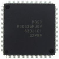
M30835FJGP#U5 Renesas Electronics America, M30835FJGP#U5 Datasheet - Page 175

M30835FJGP#U5
Manufacturer Part Number
M30835FJGP#U5
Description
IC M32C/83 MCU FLASH 144LQFP
Manufacturer
Renesas Electronics America
Series
M16C™ M32C/80r
Datasheets
1.M3087BFLGPU3.pdf
(364 pages)
2.M30833FJGPU3.pdf
(96 pages)
3.M30833FJGPU3.pdf
(529 pages)
Specifications of M30835FJGP#U5
Core Processor
M32C/80
Core Size
16/32-Bit
Speed
32MHz
Connectivity
CAN, I²C, IEBus, SIO, UART/USART
Peripherals
DMA, WDT
Number Of I /o
121
Program Memory Size
512KB (512K x 8)
Program Memory Type
FLASH
Ram Size
31K x 8
Voltage - Supply (vcc/vdd)
3 V ~ 5.5 V
Data Converters
A/D 34x10b, D/A 2x8b
Oscillator Type
Internal
Operating Temperature
-20°C ~ 85°C
Package / Case
144-LQFP
For Use With
R0K330879S001BE - KIT DEV RSK M32C/87R0K330879S000BE - KIT DEV RSK M32C/87
Lead Free Status / RoHS Status
Lead free / RoHS Compliant
Eeprom Size
-
Available stocks
Company
Part Number
Manufacturer
Quantity
Price
Part Number:
M30835FJGP#U5M30835FJGP#U3
Manufacturer:
Renesas Electronics America
Quantity:
10 000
- Current page: 175 of 529
- Download datasheet (5Mb)
R
R
M
e
E
3
. v
J
Figure 14.13 TA0MR to TA4MR Registers
2
0
1
9
C
3 .
B
8 /
0
1
3
0
3
J
G
4
a
0 -
n
o r
Timer Ai Mode Register (i=0 to 4) (Pulse Width Modulator Mode)
3 .
b7
1
u
, 1
3
NOTES:
p
1
b6
2
(
1. The MR1 bit setting is enabled only when the TAiTGH to TAiTGL bits in the TRGSR register are set
2. The CNT3 to CNT0 bits in the TCSPR register select no division (n=0) or divide-by-2n (n=1 to 15).
M
0
b5
0
to "00
TAiTGL bits are set to "01
"11
3
6
2
b4
C
2" (
8 /
Page 150
2
TAi overflow and underflow).
b3
" (input to the TAi
, 3
b2
M
3
b1
1 1
2
C
f o
b0
8 /
4
3
8
TMOD0
TMOD1
Symbol
) T
8
TCK0
TCK1
(b2)
MR1
MR2
MR3
Bit
IN
Symbol
TA0MR to TA4MR
2
pin). The MR1 bit can be set to either "0" or "1" when the TAiTGH and
" (TB2 overflow and underflow), "10
External Trigger Select
Bit
Operation Mode
Select Bit
16/8-Bit PWM Mode
Select Bit
Count Source
Select Bit
Nothing is assigned. When write, set to "0".
Trigger Select Bit
(1)
Bit Name
Address
0356
16
, 0357
16
0 : Falling edge of input signal to TAi
1 : Rising edge of input signal to TAi
b1b0
1 1 : Pulse width modulation (PWM)
0 : The TAiS bit is enabled
1 : Selected by the TAiTGH and TAiTGL
0: Functions as a 16-bit pulse width modulator
1: Functions as an 8-bit pulse width modulator
b7 b6
, 0358
0 0 : f
0 1 : f
1 0 : f
1 1 : f
bits
mode
2
" (TAi overflow and underflow) or
16
1
8
2n (2)
C32
, 0359
16
Function
, 035A
16
After Reset
0000 0X00
IN
IN
14. Timer (Timer A)
pin
pin
2
RW
RW
RW
RW
RW
RW
RW
RW
Related parts for M30835FJGP#U5
Image
Part Number
Description
Manufacturer
Datasheet
Request
R

Part Number:
Description:
KIT STARTER FOR M16C/29
Manufacturer:
Renesas Electronics America
Datasheet:

Part Number:
Description:
KIT STARTER FOR R8C/2D
Manufacturer:
Renesas Electronics America
Datasheet:

Part Number:
Description:
R0K33062P STARTER KIT
Manufacturer:
Renesas Electronics America
Datasheet:

Part Number:
Description:
KIT STARTER FOR R8C/23 E8A
Manufacturer:
Renesas Electronics America
Datasheet:

Part Number:
Description:
KIT STARTER FOR R8C/25
Manufacturer:
Renesas Electronics America
Datasheet:

Part Number:
Description:
KIT STARTER H8S2456 SHARPE DSPLY
Manufacturer:
Renesas Electronics America
Datasheet:

Part Number:
Description:
KIT STARTER FOR R8C38C
Manufacturer:
Renesas Electronics America
Datasheet:

Part Number:
Description:
KIT STARTER FOR R8C35C
Manufacturer:
Renesas Electronics America
Datasheet:

Part Number:
Description:
KIT STARTER FOR R8CL3AC+LCD APPS
Manufacturer:
Renesas Electronics America
Datasheet:

Part Number:
Description:
KIT STARTER FOR RX610
Manufacturer:
Renesas Electronics America
Datasheet:

Part Number:
Description:
KIT STARTER FOR R32C/118
Manufacturer:
Renesas Electronics America
Datasheet:

Part Number:
Description:
KIT DEV RSK-R8C/26-29
Manufacturer:
Renesas Electronics America
Datasheet:

Part Number:
Description:
KIT STARTER FOR SH7124
Manufacturer:
Renesas Electronics America
Datasheet:

Part Number:
Description:
KIT STARTER FOR H8SX/1622
Manufacturer:
Renesas Electronics America
Datasheet:

Part Number:
Description:
KIT DEV FOR SH7203
Manufacturer:
Renesas Electronics America
Datasheet:


