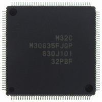
M30835FJGP#U5 Renesas Electronics America, M30835FJGP#U5 Datasheet - Page 346

M30835FJGP#U5
Manufacturer Part Number
M30835FJGP#U5
Description
IC M32C/83 MCU FLASH 144LQFP
Manufacturer
Renesas Electronics America
Series
M16C™ M32C/80r
Datasheets
1.M3087BFLGPU3.pdf
(364 pages)
2.M30833FJGPU3.pdf
(96 pages)
3.M30833FJGPU3.pdf
(529 pages)
Specifications of M30835FJGP#U5
Core Processor
M32C/80
Core Size
16/32-Bit
Speed
32MHz
Connectivity
CAN, I²C, IEBus, SIO, UART/USART
Peripherals
DMA, WDT
Number Of I /o
121
Program Memory Size
512KB (512K x 8)
Program Memory Type
FLASH
Ram Size
31K x 8
Voltage - Supply (vcc/vdd)
3 V ~ 5.5 V
Data Converters
A/D 34x10b, D/A 2x8b
Oscillator Type
Internal
Operating Temperature
-20°C ~ 85°C
Package / Case
144-LQFP
For Use With
R0K330879S001BE - KIT DEV RSK M32C/87R0K330879S000BE - KIT DEV RSK M32C/87
Lead Free Status / RoHS Status
Lead free / RoHS Compliant
Eeprom Size
-
Available stocks
Company
Part Number
Manufacturer
Quantity
Price
Part Number:
M30835FJGP#U5M30835FJGP#U3
Manufacturer:
Renesas Electronics America
Quantity:
10 000
- Current page: 346 of 529
- Download datasheet (5Mb)
M
R
R
e
E
3
. v
J
2
NOTES:
NOTES:
Table 21.42 Registers to be Used and Settings
Table 21.43 Pin Setting in Clock Synchronous Serial I/O Mode (Group 3)
Table 21.44 Pin Setting (Continued)
0
C
G3BCR0
G3BCR1
G3POCR0
G3POCR1
G3POCR2
G3PO0
G3PO2
G3FE
G3MR
G3TB
G3RB
1
9
G3CR
1. Set the MOD2 to MOD0 bits in the corresponding register to "111
1. Set the MOD2 to MOD0 bits in the corresponding register to "111
3 .
8 /
B
Name
Name
P12
P12
P12
Port
Port
P8
P8
0
1
3
Register
function used).
function used).
0
1
2
3
G
J
0
1
2
4
a
o r
0 -
n
3 .
u
1
p
, 1
3
1
ISTxD3 output
ISCLK3 input
ISCLK3 output
ISRxD3 input
(
ISTxD3 output
ISRxD3 input
2
M
0
3
0
Function
Function
2
6
C
BCK1 to BCK0
DIV4 to DIV0
IT
7 to 0
7 to 0
7 to 0
7 to 0
15 to 0
15 to 0
7 to 0
GMD1 to GMD0 Set to "01
CKDIR
TLD
UFORM
IRS
TE
TXEPT
TI
RE
RI
OPOL
IPOL
15 to 0
15 to 0
8 /
Page 321
, 3
M
Bit
3
2
C
f o
8 /
PS2_1 = 1
PS2_2 = 0
PS6 Register
PS6_0 =1
PS6_1 = 0
PS6_1 = 1
PS6_2 = 0
PS2 Register
4
3
8
) T
8
Set to "11
Select divide ratio of count source
Set to "0"
Set to "0001 0010
Set to "0000 0111
Set to "0000 0111
Set to "0000 0010
Set bit rate
Set to a value smaller than the G3PO0 register
Set to "0000 0111
Select the internal clock or external clock
Select transfer data length
Select either LSB first or MSB first
Select how the transmit interrupt is generated
Set to "1" to enable transmission
Transmit register empty flag
Transmit buffer empty flag
Set to "1" to enable reception
Receive complete flag
ISTxD3 output polarity inverse (usually set to "0")
ISRxD3 input polarity inverse
Write transmit data
Received data is stored
2 x (setting value + 2)
2
2
f
PD12_1 = 0
PD12_2 = 0
-
-
BT3
"
"
PD12 Register
PSL2_1 = 1
-
PSL2 Register
Bit and Setting
2
2
2
2
2
"
"
"
"
"
Bit and Setting
21. Intelligent I/O (Group 3 Communication Function)
= transfer clock frequency
IPS7 = 1
IPS Register
-
-
-
PD8 Register IPS Register
-
PD8_2 = 0
Function
2
2
" (output of the communication
" (output of the communication
G3POCR0
G3POCR1
-
IPS7 = 0
-
-
Register
(1)
G3POCR0
-
Register
(1)
Related parts for M30835FJGP#U5
Image
Part Number
Description
Manufacturer
Datasheet
Request
R

Part Number:
Description:
KIT STARTER FOR M16C/29
Manufacturer:
Renesas Electronics America
Datasheet:

Part Number:
Description:
KIT STARTER FOR R8C/2D
Manufacturer:
Renesas Electronics America
Datasheet:

Part Number:
Description:
R0K33062P STARTER KIT
Manufacturer:
Renesas Electronics America
Datasheet:

Part Number:
Description:
KIT STARTER FOR R8C/23 E8A
Manufacturer:
Renesas Electronics America
Datasheet:

Part Number:
Description:
KIT STARTER FOR R8C/25
Manufacturer:
Renesas Electronics America
Datasheet:

Part Number:
Description:
KIT STARTER H8S2456 SHARPE DSPLY
Manufacturer:
Renesas Electronics America
Datasheet:

Part Number:
Description:
KIT STARTER FOR R8C38C
Manufacturer:
Renesas Electronics America
Datasheet:

Part Number:
Description:
KIT STARTER FOR R8C35C
Manufacturer:
Renesas Electronics America
Datasheet:

Part Number:
Description:
KIT STARTER FOR R8CL3AC+LCD APPS
Manufacturer:
Renesas Electronics America
Datasheet:

Part Number:
Description:
KIT STARTER FOR RX610
Manufacturer:
Renesas Electronics America
Datasheet:

Part Number:
Description:
KIT STARTER FOR R32C/118
Manufacturer:
Renesas Electronics America
Datasheet:

Part Number:
Description:
KIT DEV RSK-R8C/26-29
Manufacturer:
Renesas Electronics America
Datasheet:

Part Number:
Description:
KIT STARTER FOR SH7124
Manufacturer:
Renesas Electronics America
Datasheet:

Part Number:
Description:
KIT STARTER FOR H8SX/1622
Manufacturer:
Renesas Electronics America
Datasheet:

Part Number:
Description:
KIT DEV FOR SH7203
Manufacturer:
Renesas Electronics America
Datasheet:


