M30835FJGP#U5 Renesas Electronics America, M30835FJGP#U5 Datasheet - Page 362
M30835FJGP#U5
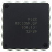
Manufacturer Part Number
M30835FJGP#U5
Description
IC M32C/83 MCU FLASH 144LQFP
Manufacturer
Renesas Electronics America
Series
M16C™ M32C/80r
Datasheets
1.M3087BFLGPU3.pdf
(364 pages)
2.M30833FJGPU3.pdf
(96 pages)
3.M30833FJGPU3.pdf
(529 pages)
Specifications of M30835FJGP#U5
Core Processor
M32C/80
Core Size
16/32-Bit
Speed
32MHz
Connectivity
CAN, I²C, IEBus, SIO, UART/USART
Peripherals
DMA, WDT
Number Of I /o
121
Program Memory Size
512KB (512K x 8)
Program Memory Type
FLASH
Ram Size
31K x 8
Voltage - Supply (vcc/vdd)
3 V ~ 5.5 V
Data Converters
A/D 34x10b, D/A 2x8b
Oscillator Type
Internal
Operating Temperature
-20°C ~ 85°C
Package / Case
144-LQFP
For Use With
R0K330879S001BE - KIT DEV RSK M32C/87R0K330879S000BE - KIT DEV RSK M32C/87
Lead Free Status / RoHS Status
Lead free / RoHS Compliant
Eeprom Size
-
Available stocks
Company
Part Number
Manufacturer
Quantity
Price

Part Number:
M30835FJGP#U5M30835FJGP#U3
Manufacturer:
Renesas Electronics America
Quantity:
10 000


R
R
M
e
E
3
. v
J
Figure 22.12 C0BRP Register
Figure 22.11 C0REC Register
2
0
22.1.9 CAN0 Receive Error Count Register (C0REC Register)
22.1.10 CAN0 Baud Rate Prescaler (C0BRP Register)
1
C
9
3 .
B
8 /
0
1
3
0
The C0BRP register determines the Tq clock cycle of the CAN bit timing. The baud rate is obtained
from Tq clock cycle x Tq per bit.
Tq: Time quantum
SS: Synchronization Segment; 1 Tq
PBS1: Phase Buffer Segment 1; 2 to 8 Tq
3
In an error active or an error passive state, a count value of the reception error is stored into the
C0REC register. The counter is decremented when the CAN module has received data as expected
or is incremented when a receive error occurs.
The C0REC register is set to 127 when the C0REC register is 128 (error passive state) or more and
the CAN module has received as expected.
In a bus-off state, an indeterminate value is stored into the C0REC register. The C0REC register is
set to "00
J
G
4
a
0 -
o r
n
Tq clock cycle = (BRP+1) / f
Baud rate =
Tq per bit = SS + PTS + PBS1 + PBS2
CAN0 Receive Error Count Register
3 .
b7
1
u
CAN0 Baud Rate Prescaler
NOTES:
b7
, 1
3
p
NOTES:
1
1. Value is obtained by setting the SLEEP bit in the C0SLPR register to "1" (sleep mode exited) and
2. Do not set to "00
2
(
M
1. Value is obtained by setting the SLEEP bit in the C0SLPR register to "1" (sleep mode exited) and
0
supplying a clock to the CAN module after reset.
16
0
3
supplying a clock to the CAN module after reset.
6
2
" when the CAN module is placed in an error active state again.
C
8 /
Page 337
, 3
M
Tq clock cycle x Tq per bit
3
2
16
C
f o
b0
" (divide-by-1).
8 /
b0
4
3
Counter Value of Receive Error
8
) T
8
If setting value is n, the CPU clock is divided
by (n+1).
Symbol
C0REC
1
1
Symbol
C0BRP
Address
020B
Address
0217
Function
BRP: Setting value of the C0BRP register; 1-255
PTS: Propagation Time Segment; 1 to 8 Tq
PBS2: Phase Buffer Segment 2; 2 to 8 Tq
16
16
Function
After Reset
00
After reset
01
16
16
Setting Range
01
(1)
(1)
16
to FF
16 (2)
22. CAN Module
RW
RO
RW
RW
Related parts for M30835FJGP#U5
Image
Part Number
Description
Manufacturer
Datasheet
Request
R

Part Number:
Description:
KIT STARTER FOR M16C/29
Manufacturer:
Renesas Electronics America
Datasheet:

Part Number:
Description:
KIT STARTER FOR R8C/2D
Manufacturer:
Renesas Electronics America
Datasheet:

Part Number:
Description:
R0K33062P STARTER KIT
Manufacturer:
Renesas Electronics America
Datasheet:

Part Number:
Description:
KIT STARTER FOR R8C/23 E8A
Manufacturer:
Renesas Electronics America
Datasheet:

Part Number:
Description:
KIT STARTER FOR R8C/25
Manufacturer:
Renesas Electronics America
Datasheet:

Part Number:
Description:
KIT STARTER H8S2456 SHARPE DSPLY
Manufacturer:
Renesas Electronics America
Datasheet:

Part Number:
Description:
KIT STARTER FOR R8C38C
Manufacturer:
Renesas Electronics America
Datasheet:

Part Number:
Description:
KIT STARTER FOR R8C35C
Manufacturer:
Renesas Electronics America
Datasheet:

Part Number:
Description:
KIT STARTER FOR R8CL3AC+LCD APPS
Manufacturer:
Renesas Electronics America
Datasheet:
Part Number:
Description:
KIT STARTER FOR RX610
Manufacturer:
Renesas Electronics America
Datasheet:

Part Number:
Description:
KIT STARTER FOR R32C/118
Manufacturer:
Renesas Electronics America
Datasheet:

Part Number:
Description:
KIT DEV RSK-R8C/26-29
Manufacturer:
Renesas Electronics America
Datasheet:

Part Number:
Description:
KIT STARTER FOR SH7124
Manufacturer:
Renesas Electronics America
Datasheet:

Part Number:
Description:
KIT STARTER FOR H8SX/1622
Manufacturer:
Renesas Electronics America
Datasheet:

Part Number:
Description:
KIT DEV FOR SH7203
Manufacturer:
Renesas Electronics America
Datasheet: