M30835FJGP#U5 Renesas Electronics America, M30835FJGP#U5 Datasheet - Page 85
M30835FJGP#U5
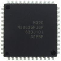
Manufacturer Part Number
M30835FJGP#U5
Description
IC M32C/83 MCU FLASH 144LQFP
Manufacturer
Renesas Electronics America
Series
M16C™ M32C/80r
Datasheets
1.M3087BFLGPU3.pdf
(364 pages)
2.M30833FJGPU3.pdf
(96 pages)
3.M30833FJGPU3.pdf
(529 pages)
Specifications of M30835FJGP#U5
Core Processor
M32C/80
Core Size
16/32-Bit
Speed
32MHz
Connectivity
CAN, I²C, IEBus, SIO, UART/USART
Peripherals
DMA, WDT
Number Of I /o
121
Program Memory Size
512KB (512K x 8)
Program Memory Type
FLASH
Ram Size
31K x 8
Voltage - Supply (vcc/vdd)
3 V ~ 5.5 V
Data Converters
A/D 34x10b, D/A 2x8b
Oscillator Type
Internal
Operating Temperature
-20°C ~ 85°C
Package / Case
144-LQFP
For Use With
R0K330879S001BE - KIT DEV RSK M32C/87R0K330879S000BE - KIT DEV RSK M32C/87
Lead Free Status / RoHS Status
Lead free / RoHS Compliant
Eeprom Size
-
Available stocks
Company
Part Number
Manufacturer
Quantity
Price

Part Number:
M30835FJGP#U5M30835FJGP#U3
Manufacturer:
Renesas Electronics America
Quantity:
10 000


R
R
M
e
E
3
. v
J
Figure 7.4 External Bus Operation with Software Wait State (1)
2
0
C
1
9
3 .
B
8 /
0
1
3
0
(3) Separate Bus with 2 Wait States
3
(1) Separate Bus with No Wait State
(2) Separate Bus with 1 Wait State
J
G
4
a
NOTES:
o r
0 -
n
BCLK
Address Bus
Write Signal
Read Signal
Data Bus
Chip-Select Signal
Read Signal
Data Bus
Chip-Select Signal
Chip-Select Signal
BCLK
Write Signal
Address Bus
3 .
BCLK
Write Signal
Data Bus
Address Bus
1
u
Read Signal
1. This example illustrates bus cycle length. Read cycle and write cycle may occur consecutively.
2. The address bus and chip-select signal may be extended depending on CPU state such as an
3. When the microcomputer continuously accesses the same external space (same CS area), the chip-
, 1
3
p
1
instruction queue buffer.
select signal may be output continuously.
(
2
M
0
0
3
6
2
C
(2)
8 /
(2)
(2)
Page 60
, 3
M
(2, 3)
(2, 3)
(2, 3)
3
2
C
f o
8 /
4
3
8
) T
8
Address
Bus cycle
Data Output
Bus cycle
Bus cycle
Address
Address
(1)
Output
Output
(1)
(1)
Bus cycle
Address
Input
(1)
Bus cycle
Address
Bus cycle
Address
(1)
(1)
Input
Input
7. Bus
Related parts for M30835FJGP#U5
Image
Part Number
Description
Manufacturer
Datasheet
Request
R

Part Number:
Description:
KIT STARTER FOR M16C/29
Manufacturer:
Renesas Electronics America
Datasheet:

Part Number:
Description:
KIT STARTER FOR R8C/2D
Manufacturer:
Renesas Electronics America
Datasheet:

Part Number:
Description:
R0K33062P STARTER KIT
Manufacturer:
Renesas Electronics America
Datasheet:

Part Number:
Description:
KIT STARTER FOR R8C/23 E8A
Manufacturer:
Renesas Electronics America
Datasheet:

Part Number:
Description:
KIT STARTER FOR R8C/25
Manufacturer:
Renesas Electronics America
Datasheet:

Part Number:
Description:
KIT STARTER H8S2456 SHARPE DSPLY
Manufacturer:
Renesas Electronics America
Datasheet:

Part Number:
Description:
KIT STARTER FOR R8C38C
Manufacturer:
Renesas Electronics America
Datasheet:

Part Number:
Description:
KIT STARTER FOR R8C35C
Manufacturer:
Renesas Electronics America
Datasheet:

Part Number:
Description:
KIT STARTER FOR R8CL3AC+LCD APPS
Manufacturer:
Renesas Electronics America
Datasheet:
Part Number:
Description:
KIT STARTER FOR RX610
Manufacturer:
Renesas Electronics America
Datasheet:

Part Number:
Description:
KIT STARTER FOR R32C/118
Manufacturer:
Renesas Electronics America
Datasheet:

Part Number:
Description:
KIT DEV RSK-R8C/26-29
Manufacturer:
Renesas Electronics America
Datasheet:

Part Number:
Description:
KIT STARTER FOR SH7124
Manufacturer:
Renesas Electronics America
Datasheet:

Part Number:
Description:
KIT STARTER FOR H8SX/1622
Manufacturer:
Renesas Electronics America
Datasheet:

Part Number:
Description:
KIT DEV FOR SH7203
Manufacturer:
Renesas Electronics America
Datasheet: