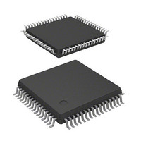
DF36037FZJV Renesas Electronics America, DF36037FZJV Datasheet - Page 246

DF36037FZJV
Manufacturer Part Number
DF36037FZJV
Description
MCU 3/5V 56K PB-FREE J-TEMP 64-L
Manufacturer
Renesas Electronics America
Series
H8® H8/300H Tinyr
Datasheet
1.DF36057GFZV.pdf
(594 pages)
Specifications of DF36037FZJV
Core Processor
H8/300H
Core Size
16-Bit
Speed
20MHz
Connectivity
CAN, SCI, SSU
Peripherals
PWM, WDT
Number Of I /o
45
Program Memory Size
56KB (56K x 8)
Program Memory Type
FLASH
Ram Size
3K x 8
Voltage - Supply (vcc/vdd)
3 V ~ 5.5 V
Data Converters
A/D 8x10b
Oscillator Type
Internal
Operating Temperature
-40°C ~ 85°C
Package / Case
64-LQFP
For Use With
R0K436079S000BE - KIT DEV FOR H8/36079 W/COMPILER
Lead Free Status / RoHS Status
Lead free / RoHS Compliant
Eeprom Size
-
- Current page: 246 of 594
- Download datasheet (4Mb)
Section 12 Timer Z
Rev. 4.00 Mar. 15, 2006 Page 212 of 556
REJ09B0026-0400
<Complementary PWM mode>
Note: To re-enter complementary PWM mode, first, enter a mode other than the complementary
Complementary PWM mode
Enable waveform output
Figure 12.29 Example of Complementary PWM Mode Setting Procedure
Stop counter operation
Start counter operation
Select counter clock
Initialize output pin
Set complementary
Initialize output pin
PWM mode. After that, repeat the setting procedures from step [1].
For settings of waveform outputs with a duty cycle of 0% and 100%, see Examples of
Complementary PWM Mode Operation and Setting GR Value in Complementary PWM
Mode in section 12.4.7, Complementary PWM Mode.
PWM mode
Set TCNT
Set GR
[1]
[2]
[3]
[4]
[5]
[6]
[7]
[8]
[9]
[1] Clear bits STR0 and STR1 in TSTR to 0,
[2] Write H'00 to TOCR.
[3] Use bits TPSC2 to TPSC0 in TCR to
[4] Use bits CMD1 and CMD0 in TFCR to set
[5] Set H'00 to TOCR.
[6] TCNT_1 must be H'0000. Set a non-
[7] GRA_0 is a cycle register. Set the cycle to
[8] Use TOER to enable or disable the timer
[9] Set the STR0 and STR1 bits in TSTR to 1
and stop the counter operation of
TCNT_0. Stop TCNT_0 and TCNT_1 and
set complementary PWM mode.
select the same counter clock for channels
0 and 1. When an external clock is
selected, select the edge of the external
clock by bits CKEG1 and CKEG0 in TCR.
Do not use bits CCLR1 and CCLR0 in
TCR to clear the counter.
complementary PWM mode. FTIOB0 to
FTIOD0 and FTIOA1 to FTIOD1
automatically become PWM output pins.
overlapped period to TCNT_0.
GRA_0. Set the timing to change the
PWM output waveform to GRB_0, GRA_1,
and GRB_1. Note that the timing must be
set within the range of compare match
carried out for TCNT_0 and TCNT_1.
For GR settings, see Setting GR Value in
Complementary PWM Mode in section
12.4.7, Complementary PWM Mode.
output.
to start the count operation.
Related parts for DF36037FZJV
Image
Part Number
Description
Manufacturer
Datasheet
Request
R

Part Number:
Description:
Headers & Wire Housings 20P PLUG METAL COVER
Manufacturer:
Hirose Electric Co Ltd

Part Number:
Description:
Headers & Wire Housings 25P PLUG METAL COVER
Manufacturer:
Hirose Electric Co Ltd

Part Number:
Description:
Headers & Wire Housings 15P PLUG METAL COVER
Manufacturer:
Hirose Electric Co Ltd

Part Number:
Description:
0.4 Mm Pitch, 1.5 Mm Mated Height, Board-to-fine Coaxial Cable Connectors
Manufacturer:
Hirose Electric
Datasheet:

Part Number:
Description:
CONN RECEPT 40POS 0.4MM SMD GOLD
Manufacturer:
Hirose Electric Co Ltd
Datasheet:

Part Number:
Description:
KIT STARTER FOR M16C/29
Manufacturer:
Renesas Electronics America
Datasheet:

Part Number:
Description:
KIT STARTER FOR R8C/2D
Manufacturer:
Renesas Electronics America
Datasheet:

Part Number:
Description:
R0K33062P STARTER KIT
Manufacturer:
Renesas Electronics America
Datasheet:

Part Number:
Description:
KIT STARTER FOR R8C/23 E8A
Manufacturer:
Renesas Electronics America
Datasheet:

Part Number:
Description:
KIT STARTER FOR R8C/25
Manufacturer:
Renesas Electronics America
Datasheet:

Part Number:
Description:
KIT STARTER H8S2456 SHARPE DSPLY
Manufacturer:
Renesas Electronics America
Datasheet:

Part Number:
Description:
KIT STARTER FOR R8C38C
Manufacturer:
Renesas Electronics America
Datasheet:

Part Number:
Description:
KIT STARTER FOR R8C35C
Manufacturer:
Renesas Electronics America
Datasheet:

Part Number:
Description:
KIT STARTER FOR R8CL3AC+LCD APPS
Manufacturer:
Renesas Electronics America
Datasheet:

Part Number:
Description:
KIT STARTER FOR RX610
Manufacturer:
Renesas Electronics America
Datasheet:


