R5F2121AJFP#U0 Renesas Electronics America, R5F2121AJFP#U0 Datasheet - Page 13
R5F2121AJFP#U0
Manufacturer Part Number
R5F2121AJFP#U0
Description
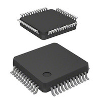
MCU FLASH 96K 5K CMOS 48-LQFP
Manufacturer
Renesas Electronics America
Series
R8C/2x/21r
Datasheet
1.R5F21216JFP.pdf
(503 pages)
Specifications of R5F2121AJFP#U0
Core Processor
R8C
Core Size
16/32-Bit
Speed
20MHz
Connectivity
I²C, LIN, SIO, SSU, UART/USART
Peripherals
POR, Voltage Detect, WDT
Number Of I /o
41
Program Memory Size
96KB (96K x 8)
Program Memory Type
FLASH
Ram Size
5K x 8
Voltage - Supply (vcc/vdd)
2.7 V ~ 5.5 V
Data Converters
A/D 12x10b
Oscillator Type
Internal
Operating Temperature
-40°C ~ 85°C
Package / Case
48-LQFP
Lead Free Status / RoHS Status
Lead free / RoHS Compliant
Eeprom Size
-
Available stocks
Company
Part Number
Manufacturer
Quantity
Price


15.
16.
17.
18.
15.1
15.2
15.3
16.1
16.2
16.3
17.1
17.2
17.3
17.4
17.5
17.6
18.1
18.2
18.3
14.4.1
14.4.2
15.1.1
15.1.2
15.1.3
15.2.1
16.2.1
16.2.2
16.2.3
16.2.4
16.2.5
16.2.6
16.2.7
16.2.8
16.3.1
16.3.2
16.3.3
16.3.4
16.3.5
16.3.6
16.3.7
16.3.8
17.4.1
17.4.2
17.4.3
17.4.4
Serial Interface ............................................................................................................................ 265
Clock Synchronous Serial Interface ............................................................................................ 282
Hardware LIN .............................................................................................................................. 345
A/D Converter ............................................................................................................................. 360
Clock Synchronous Serial I/O Mode ..................................................................................................... 271
Clock Asynchronous Serial I/O (UART) Mode .................................................................................... 276
Notes on Serial Interface ....................................................................................................................... 281
Mode Selection ...................................................................................................................................... 282
Clock Synchronous Serial I/O with Chip Select (SSU) ........................................................................ 283
I
Features ................................................................................................................................................. 345
Input/Output Pins .................................................................................................................................. 346
Register Configuration .......................................................................................................................... 347
Functional Description .......................................................................................................................... 349
Interrupt Requests .................................................................................................................................. 358
Notes on Hardware LIN ........................................................................................................................ 359
One-Shot Mode ..................................................................................................................................... 364
Repeat Mode .......................................................................................................................................... 367
Sample and Hold ................................................................................................................................... 370
2
C Bus Interface ................................................................................................................................... 312
Output Compare Mode ..................................................................................................................... 258
Notes on Timer RE ........................................................................................................................... 264
Polarity Select Function .................................................................................................................... 274
LSB First/MSB First Select Function ............................................................................................... 274
Continuous Receive Mode ................................................................................................................ 275
Bit Rate ............................................................................................................................................. 280
Transfer Clock .................................................................................................................................. 292
SS Shift Register (SSTRSR) ............................................................................................................. 294
Interrupt Requests ............................................................................................................................. 295
Communication Modes and Pin Functions ....................................................................................... 296
Clock Synchronous Communication Mode ...................................................................................... 297
Operation in 4-Wire Bus Communication Mode .............................................................................. 304
SCS Pin Control and Arbitration ...................................................................................................... 310
Notes on Clock Synchronous Serial I/O with Chip Select ............................................................... 311
Transfer Clock .................................................................................................................................. 322
Interrupt Requests ............................................................................................................................. 323
I
Clock Synchronous Serial Mode ...................................................................................................... 335
Noise Canceller ................................................................................................................................. 338
Bit Synchronization Circuit .............................................................................................................. 339
Examples of Register Setting ............................................................................................................ 340
Notes on I
Master Mode ..................................................................................................................................... 349
Slave Mode ....................................................................................................................................... 352
Bus Collision Detection Function ..................................................................................................... 356
Hardware LIN End Processing ......................................................................................................... 357
2
C Bus Interface Mode .................................................................................................................... 324
2
C Bus Interface ............................................................................................................... 344
A - 4
Related parts for R5F2121AJFP#U0
Image
Part Number
Description
Manufacturer
Datasheet
Request
R

Part Number:
Description:
KIT STARTER FOR M16C/29
Manufacturer:
Renesas Electronics America
Datasheet:

Part Number:
Description:
KIT STARTER FOR R8C/2D
Manufacturer:
Renesas Electronics America
Datasheet:

Part Number:
Description:
R0K33062P STARTER KIT
Manufacturer:
Renesas Electronics America
Datasheet:

Part Number:
Description:
KIT STARTER FOR R8C/23 E8A
Manufacturer:
Renesas Electronics America
Datasheet:

Part Number:
Description:
KIT STARTER FOR R8C/25
Manufacturer:
Renesas Electronics America
Datasheet:

Part Number:
Description:
KIT STARTER H8S2456 SHARPE DSPLY
Manufacturer:
Renesas Electronics America
Datasheet:

Part Number:
Description:
KIT STARTER FOR R8C38C
Manufacturer:
Renesas Electronics America
Datasheet:

Part Number:
Description:
KIT STARTER FOR R8C35C
Manufacturer:
Renesas Electronics America
Datasheet:

Part Number:
Description:
KIT STARTER FOR R8CL3AC+LCD APPS
Manufacturer:
Renesas Electronics America
Datasheet:
Part Number:
Description:
KIT STARTER FOR RX610
Manufacturer:
Renesas Electronics America
Datasheet:

Part Number:
Description:
KIT STARTER FOR R32C/118
Manufacturer:
Renesas Electronics America
Datasheet:

Part Number:
Description:
KIT DEV RSK-R8C/26-29
Manufacturer:
Renesas Electronics America
Datasheet:

Part Number:
Description:
KIT STARTER FOR SH7124
Manufacturer:
Renesas Electronics America
Datasheet:

Part Number:
Description:
KIT STARTER FOR H8SX/1622
Manufacturer:
Renesas Electronics America
Datasheet:

Part Number:
Description:
KIT DEV FOR SH7203
Manufacturer:
Renesas Electronics America
Datasheet: