AT91M55800A-33CJ Atmel, AT91M55800A-33CJ Datasheet - Page 191
AT91M55800A-33CJ
Manufacturer Part Number
AT91M55800A-33CJ
Description
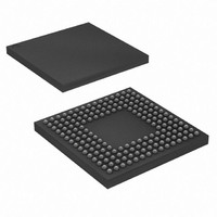
IC ARM MCU 16BIT 176BGA
Manufacturer
Atmel
Series
AT91SAMr
Specifications of AT91M55800A-33CJ
Core Processor
ARM7
Core Size
16/32-Bit
Speed
33MHz
Connectivity
EBI/EMI, SPI, UART/USART
Peripherals
POR, WDT
Number Of I /o
58
Program Memory Type
ROMless
Ram Size
8K x 8
Voltage - Supply (vcc/vdd)
2.7 V ~ 3.6 V
Data Converters
A/D 8x10b; D/A 2x10b
Oscillator Type
Internal
Operating Temperature
-40°C ~ 85°C
Package / Case
176-LFBGA
Processor Series
AT91Mx
Core
ARM7TDMI
Data Bus Width
32 bit
Data Ram Size
8 KB
Interface Type
EBI, SPI, USART
Maximum Clock Frequency
33 MHz
Number Of Programmable I/os
58
Number Of Timers
10 bit
Operating Supply Voltage
3 V to 3.6 V
Maximum Operating Temperature
+ 85 C
Mounting Style
SMD/SMT
3rd Party Development Tools
JTRACE-ARM-2M, MDK-ARM, RL-ARM, ULINK2
Development Tools By Supplier
AT91EB55
Minimum Operating Temperature
- 40 C
On-chip Adc
10 bit, 8 Channel
On-chip Dac
8 bit, 2 Channel
Cpu Family
AT91
Device Core
ARM7TDMI
Device Core Size
32b
Frequency (max)
33MHz
Program Memory Size
Not Required
Total Internal Ram Size
8KB
# I/os (max)
58
Number Of Timers - General Purpose
6
Operating Supply Voltage (typ)
3.3V
Operating Supply Voltage (max)
3.6V
Operating Supply Voltage (min)
2.7V
Instruction Set Architecture
RISC
Operating Temp Range
-40C to 85C
Operating Temperature Classification
Industrial
Mounting
Surface Mount
Pin Count
176
Package Type
BGA
For Use With
AT91EB55 - KIT EVAL FOR ARM AT91M55800A
Lead Free Status / RoHS Status
Contains lead / RoHS non-compliant
Eeprom Size
-
Program Memory Size
-
Lead Free Status / Rohs Status
Lead free / RoHS Compliant
Available stocks
Company
Part Number
Manufacturer
Quantity
Price
Company:

Part Number:
AT91M55800A-33CJ
Manufacturer:
ATMEL
Quantity:
590
Part Number:
AT91M55800A-33CJ
Manufacturer:
ATMEL/爱特梅尔
Quantity:
20 000
Company:
Part Number:
AT91M55800A-33CJ SL383
Manufacturer:
Atmel
Quantity:
10 000


Table 20-1.
Notes:
20.2
20.2.1
1745F–ATARM–06-Sep-07
Pin Name
Master In Slave Out
Master Out Slave In
Serial Clock
Peripheral Chip Selects
Peripheral Chip Select/
Slave Select
1. After a hardware reset, the SPI clock is disabled by default. The user must configure the Power Management Controller
2. After a hardware reset, the SPI pins are deselected by default (see
Master Mode
Fixed Peripheral Select
before any access to the User Interface of the SPI.
The user must configure the PIO Controller to enable the corresponding pins for their SPI function. NPCS0/NSS must be
configured as open drain in the Parallel I/O Controller for multi-master operation.
SPI Pins
In Master Mode, the SPI controls data transfers to and from the slave(s) connected to the SPI
bus. The SPI drives the chip select(s) to the slave(s) and the serial clock (SPCK). After enabling
the SPI, a data transfer begins when the ARM core writes to the SP_TDR (Transmit Data
Register).
Transmit and Receive buffers maintain the data flow at a constant rate with a reduced require-
ment for high priority interrupt servicing. When new data is available in the SP_TDR (Transmit
Data Register) the SPI continues to transfer data. If the SP_RDR (Receive Data Register) has
not been read before new data is received, the Overrun Error (OVRES) flag is set.
The delay between the activation of the chip select and the start of the data transfer (DLYBS) as
well as the delay between each data transfer (DLYBCT) can be programmed for each of the four
external chip selects. All data transfer characteristics including the two timing values are pro-
grammed in registers SP_CSR0 to SP_CSR3 (Chip Select Registers). See
In master mode the peripheral selection can be defined in two different ways:
Figures 20-2 and 20-3 show the operation of the SPI in Master Mode. For details concerning the
flag and control bits in these diagrams, see the tables in the Programmer’s Model, starting on
page 198.
This mode is ideal for transferring memory blocks without the extra overhead in the transmit data
register to determine the peripheral.
Fixed Peripheral Select is activated by setting bit PS to zero in SP_MR (Mode Register). The
peripheral is defined by the PCS field, also in SP_MR.
This option is only available when the SPI is programmed in master mode.
• Fixed Peripheral Select: SPI exchanges data with only one peripheral
• Variable Peripheral Select: Data can be exchanged with more than one peripheral
Mnemonic
NPCS[3:1]
NPCS0/
SPCK
MISO
MOSI
NSS
Master
Master
Master
Master
Master
Master
Mode
Slave
Slave
Slave
Slave
Function
Serial data input to SPI
Serial data output from SPI
Serial data output from SPI
Serial data input to SPI
Clock output from SPI
Clock input to SPI
Select peripherals
Output: Selects peripheral
Input: low causes mode fault
Input: chip select for SPI
Section 16. “PIO: Parallel I/O Controller” on page
AT91M5880A
Table
20-2.
113).
191
Related parts for AT91M55800A-33CJ
Image
Part Number
Description
Manufacturer
Datasheet
Request
R

Part Number:
Description:
IC ARM7 MCU 176 TQFP
Manufacturer:
Atmel
Datasheet:

Part Number:
Description:
IC ARM7 MCU 176 BGA
Manufacturer:
Atmel
Datasheet:

Part Number:
Description:
DEV KIT FOR AVR/AVR32
Manufacturer:
Atmel
Datasheet:

Part Number:
Description:
INTERVAL AND WIPE/WASH WIPER CONTROL IC WITH DELAY
Manufacturer:
ATMEL Corporation
Datasheet:
Part Number:
Description:
Low-Voltage Voice-Switched IC for Hands-Free Operation
Manufacturer:
ATMEL Corporation
Datasheet:
Part Number:
Description:
MONOLITHIC INTEGRATED FEATUREPHONE CIRCUIT
Manufacturer:
ATMEL Corporation
Datasheet:
Part Number:
Description:
AM-FM Receiver IC U4255BM-M
Manufacturer:
ATMEL Corporation
Datasheet:
Part Number:
Description:
Monolithic Integrated Feature Phone Circuit
Manufacturer:
ATMEL Corporation
Datasheet:
Part Number:
Description:
Multistandard Video-IF and Quasi Parallel Sound Processing
Manufacturer:
ATMEL Corporation
Datasheet:
Part Number:
Description:
High-performance EE PLD
Manufacturer:
ATMEL Corporation
Datasheet:
Part Number:
Description:
8-bit Flash Microcontroller
Manufacturer:
ATMEL Corporation
Datasheet:
Part Number:
Description:
2-Wire Serial EEPROM
Manufacturer:
ATMEL Corporation
Datasheet: