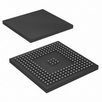
AT91SAM9260B-CU-999 Atmel, AT91SAM9260B-CU-999 Datasheet - Page 782

AT91SAM9260B-CU-999
Manufacturer Part Number
AT91SAM9260B-CU-999
Description
IC MCU ARM9 217LFBGA
Manufacturer
Atmel
Series
AT91SAMr
Datasheet
1.AT91SAM9260B-CU-999.pdf
(798 pages)
Specifications of AT91SAM9260B-CU-999
Core Processor
ARM9
Core Size
16/32-Bit
Speed
180MHz
Connectivity
EBI/EMI, Ethernet, I²C, MMC, SPI, SSC, UART/USART, USB
Peripherals
POR, WDT
Number Of I /o
96
Program Memory Size
32KB (32K x 8)
Program Memory Type
ROM
Ram Size
24K x 8
Voltage - Supply (vcc/vdd)
1.65 V ~ 1.95 V
Data Converters
A/D 4x10b
Oscillator Type
Internal
Operating Temperature
-40°C ~ 85°C
Package / Case
217-LFBGA
Processor Series
AT91SAMx
Core
ARM926EJ-S
Data Bus Width
32 bit
Data Ram Size
8 KB
Interface Type
2-Wire, EBI, I2S, SPI, USART
Maximum Clock Frequency
180 MHz
Number Of Programmable I/os
96
Number Of Timers
6
Maximum Operating Temperature
+ 85 C
Mounting Style
SMD/SMT
3rd Party Development Tools
JTRACE-ARM-2M, MDK-ARM, RL-ARM, ULINK2
Development Tools By Supplier
AT91SAM-ICE, AT91-ISP, AT91SAM9260-EK
Minimum Operating Temperature
- 40 C
On-chip Adc
10 bit, 4 Channel
For Use With
AT91SAM9260-EK - KIT EVAL FOR AT91SAM9260AT91SAM-ICE - EMULATOR FOR AT91 ARM7/ARM9
Lead Free Status / RoHS Status
Lead free / RoHS Compliant
Eeprom Size
-
Lead Free Status / Rohs Status
Details
Available stocks
Company
Part Number
Manufacturer
Quantity
Price
- Current page: 782 of 798
- Download datasheet (12Mb)
782
Revision
6221F (Cont)
AT91SAM9260
Comments
UDP:
In the USB_CSR register, the control endpoints are not effected by the bit field,
Enable Disable” on page
Updated: write 1 =.... in
Updated: write 0 =....in
Section 36.7.10 “UDP Endpoint Control and Status Register” on page
instructions regarding USB clock and system clock cycle, and updated “note” appearing under the
code. “wait 3 USB clock cycles and 3 system clock cycles before accessing DPR from RX_DATAx and
TXPKTRDY bit fields, ditto for RX_DATAx and TXPKTRDY bit field descriptions.”
Section 36.3 “Block Diagram” on page
clock used by Master Clock domain, UDPCK specified as 48 MHz clock used by 12 MHz domain, in
peripheral clock requirements.
Section 36.7 “USB Device Port (UDP) User Interface” on page
been updated.
Section 36.7.6 “UDP Interrupt Mask Register” on page 656
cannot be masked.
ADC: New widths for fields PRESCAL and STARTUP in
715.
In
VIL, VIH, VOL, VOH lines updated with 1.8V conditions
In
Characteristics,” on page
In
Capacitance with a CCRYSTAL = 12.5 pF
Corrected R
Corrected values in
Section 42.1, “Thermal Conditions” removed.
Corrected package reference to PQFP in
778.
Updated BGA ordering code in
Errata: Added ADC errata,
44.2.1.11 ”ADC: Sleep Mode” on page
In
constraint” on page
In
on second chip_select when SCBR = 1, CPOL = 1 and NCPHA = 0” on page
In
cycle when RK outputs a clock during data transfer” on page 787
when RK outputs a clock during data transfer” on page
Added
Added
In
Handshaking mod.” on page 789
Table 40-2, “DC Characteristics,” on page
Section 41.5 ”Crystal Oscillator Characteristics” on page
Table 40-11, “Main Oscillator Characteristics,” on page
Section 44.2.7 ”SDRAM Controller” on page
Section 44.2.8 ”Serial Peripheral Interface (SPI)” on page
Section 44.2.9 ”Serial Synchronous Controller (SSC)” on page
Section 44.2.13 ”USART” on page
Table 36-2, “USB Communication
Section 43.2.5 “I/O Considerations” on page
Section 44.2.11 ”Two-wire Interface (TWI)” on page
EXT
value in
Table 40-22, “SDRAMC Clock Signal,” on page
786.
“TXPKTRDY: Transmit Packet Ready”
“RX_DATA_BK0: Receive Data Bank 0”
Figure 41-12, ”USB Data Signal Rise and Fall Times” on page
666.
754.
Section 44.2.1.1 ”ADC: DRDY Bit Cleared” on page 782
Section 43. ”AT91SAM9260 Ordering Information” on page
and
789, added
“DCD is Active High instead of Low” on page
632, in the text below the block diagram, MCK specified as
783.
Flow”, Supported Endpoint column updated.
Figure 42-2, ”208-lead PQFP Package Drawing” on page
725, added typ values for power supply parameters.
786, updated
“TXD signal is floating in Modem and Hardware
759.
787.
Section 39.7.2 “ADC Mode Register” on page
731, corrected typ value of External Load
bit 12 has been defined as BIT12 and
754, added
788.
786, added
“Mobile SDRAM device initialization
649, the register mapping table has
bit field of USB_CSR register.
bit field of USB_CSR register.
787, added
and
739.
662, update to code and added
“Incorrect first RK clock cycle
Table 41-10, “Crystal
“Bad Serial Clock Generation
“Unexpected RK clock
786.
“EPEDS: Endpoint
789.
to
Section
774.
780.
6221I–ATARM–17-Jul-09
Change
Request
Ref.
3476
4063
4099
4462
4487
4508
4802
4430
5002
4929
4837
4974
4627
5084
4728
4740
4768
4718
4637
4769
4980
4691
4720
Related parts for AT91SAM9260B-CU-999
Image
Part Number
Description
Manufacturer
Datasheet
Request
R

Part Number:
Description:
Manufacturer:
ATMEL Corporation
Datasheet:

Part Number:
Description:
KIT EVAL FOR AT91SAM9260
Manufacturer:
Atmel
Datasheet:

Part Number:
Description:
AT91 ARM Thumb Microcontrollers
Manufacturer:
ATMEL [ATMEL Corporation]
Datasheet:

Part Number:
Description:
AT91 ARM Thumb Microcontrollers
Manufacturer:
ATMEL Corporation
Datasheet:

Part Number:
Description:
At91 Arm Thumb Microcontrollers
Manufacturer:
ATMEL Corporation
Datasheet:

Part Number:
Description:
MCU, MPU & DSP Development Tools DEV BRD FOR AT91SAM9260
Manufacturer:
Olimex Ltd.
Datasheet:

Part Number:
Description:
MCU, MPU & DSP Development Tools KICKSTART KIT FOR AT91SAM9 PLUS
Manufacturer:
IAR Systems

Part Number:
Description:
DEV KIT FOR AVR/AVR32
Manufacturer:
Atmel
Datasheet:

Part Number:
Description:
INTERVAL AND WIPE/WASH WIPER CONTROL IC WITH DELAY
Manufacturer:
ATMEL Corporation
Datasheet:

Part Number:
Description:
Low-Voltage Voice-Switched IC for Hands-Free Operation
Manufacturer:
ATMEL Corporation
Datasheet:

Part Number:
Description:
MONOLITHIC INTEGRATED FEATUREPHONE CIRCUIT
Manufacturer:
ATMEL Corporation
Datasheet:

Part Number:
Description:
AM-FM Receiver IC U4255BM-M
Manufacturer:
ATMEL Corporation
Datasheet:

Part Number:
Description:
Monolithic Integrated Feature Phone Circuit
Manufacturer:
ATMEL Corporation
Datasheet:

Part Number:
Description:
Multistandard Video-IF and Quasi Parallel Sound Processing
Manufacturer:
ATMEL Corporation
Datasheet:


