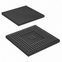
AT91SAM9260B-CU-999 Atmel, AT91SAM9260B-CU-999 Datasheet - Page 405

AT91SAM9260B-CU-999
Manufacturer Part Number
AT91SAM9260B-CU-999
Description
IC MCU ARM9 217LFBGA
Manufacturer
Atmel
Series
AT91SAMr
Datasheet
1.AT91SAM9260B-CU-999.pdf
(798 pages)
Specifications of AT91SAM9260B-CU-999
Core Processor
ARM9
Core Size
16/32-Bit
Speed
180MHz
Connectivity
EBI/EMI, Ethernet, I²C, MMC, SPI, SSC, UART/USART, USB
Peripherals
POR, WDT
Number Of I /o
96
Program Memory Size
32KB (32K x 8)
Program Memory Type
ROM
Ram Size
24K x 8
Voltage - Supply (vcc/vdd)
1.65 V ~ 1.95 V
Data Converters
A/D 4x10b
Oscillator Type
Internal
Operating Temperature
-40°C ~ 85°C
Package / Case
217-LFBGA
Processor Series
AT91SAMx
Core
ARM926EJ-S
Data Bus Width
32 bit
Data Ram Size
8 KB
Interface Type
2-Wire, EBI, I2S, SPI, USART
Maximum Clock Frequency
180 MHz
Number Of Programmable I/os
96
Number Of Timers
6
Maximum Operating Temperature
+ 85 C
Mounting Style
SMD/SMT
3rd Party Development Tools
JTRACE-ARM-2M, MDK-ARM, RL-ARM, ULINK2
Development Tools By Supplier
AT91SAM-ICE, AT91-ISP, AT91SAM9260-EK
Minimum Operating Temperature
- 40 C
On-chip Adc
10 bit, 4 Channel
For Use With
AT91SAM9260-EK - KIT EVAL FOR AT91SAM9260AT91SAM-ICE - EMULATOR FOR AT91 ARM7/ARM9
Lead Free Status / RoHS Status
Lead free / RoHS Compliant
Eeprom Size
-
Lead Free Status / Rohs Status
Details
Available stocks
Company
Part Number
Manufacturer
Quantity
Price
- Current page: 405 of 798
- Download datasheet (12Mb)
Figure 30-24. Read Access Ordered by a MASTER
Notes:
30.10.5.2
Figure 30-25. Write Access Ordered by a Master
Notes:
405
EOSVACC
EOSVACC
SVREAD
SVREAD
SVACC
RXRDY
TXRDY
SVACC
NACK
1. When SVACC is low, the state of SVREAD becomes irrelevant.
2. TXRDY is reset when data has been transmitted from TWI_THR to the shift register and set when this data has been
1. When SVACC is low, the state of SVREAD becomes irrelevant.
2. RXRDY is set when data has been transmitted from the shift register to the TWI_RHR and reset when this data is read.
TWD
TWD
AT91SAM9260
acknowledged or non acknowledged.
Write Operation
S
S
ADR
ADR
TWI answers with a NACK
TWI answers with a NACK
SADR does not match,
SADR does not match,
The write mode is defined as a data transmission from the master.
After a START or a REPEATED START, the decoding of the address starts. If the slave address
is decoded, SVACC is set and SVREAD indicates the direction of the transfer (SVREAD is low in
this case).
Until a STOP or REPEATED START condition is detected, TWI stores the received data in the
TWI_RHR register.
If a STOP condition or a REPEATED START + an address different from SADR is detected,
SVACC is reset.
Figure 30-25 on page 405
W
R
NA
NA
DATA
DATA
NA
NA
P/S/Sr
P/S/Sr
describes the Write operation.
Write THR
SADR
SADR
TWI answers with an ACK
TWI answers with an ACK
SADR matches,
SADR matches,
W A
R
SVREAD has to be taken into account only while SVACC is active
SVREAD has to be taken into account only while SVACC is active
A
DATA
DATA
A
A
Read RHR
ACK/NACK from the Master
A
A
DATA NA S/Sr
DATA
NA
6221I–ATARM–17-Jul-09
S/Sr
Read RHR
Related parts for AT91SAM9260B-CU-999
Image
Part Number
Description
Manufacturer
Datasheet
Request
R

Part Number:
Description:
Manufacturer:
ATMEL Corporation
Datasheet:

Part Number:
Description:
KIT EVAL FOR AT91SAM9260
Manufacturer:
Atmel
Datasheet:

Part Number:
Description:
AT91 ARM Thumb Microcontrollers
Manufacturer:
ATMEL [ATMEL Corporation]
Datasheet:

Part Number:
Description:
AT91 ARM Thumb Microcontrollers
Manufacturer:
ATMEL Corporation
Datasheet:

Part Number:
Description:
At91 Arm Thumb Microcontrollers
Manufacturer:
ATMEL Corporation
Datasheet:

Part Number:
Description:
MCU, MPU & DSP Development Tools DEV BRD FOR AT91SAM9260
Manufacturer:
Olimex Ltd.
Datasheet:

Part Number:
Description:
MCU, MPU & DSP Development Tools KICKSTART KIT FOR AT91SAM9 PLUS
Manufacturer:
IAR Systems

Part Number:
Description:
DEV KIT FOR AVR/AVR32
Manufacturer:
Atmel
Datasheet:

Part Number:
Description:
INTERVAL AND WIPE/WASH WIPER CONTROL IC WITH DELAY
Manufacturer:
ATMEL Corporation
Datasheet:

Part Number:
Description:
Low-Voltage Voice-Switched IC for Hands-Free Operation
Manufacturer:
ATMEL Corporation
Datasheet:

Part Number:
Description:
MONOLITHIC INTEGRATED FEATUREPHONE CIRCUIT
Manufacturer:
ATMEL Corporation
Datasheet:

Part Number:
Description:
AM-FM Receiver IC U4255BM-M
Manufacturer:
ATMEL Corporation
Datasheet:

Part Number:
Description:
Monolithic Integrated Feature Phone Circuit
Manufacturer:
ATMEL Corporation
Datasheet:

Part Number:
Description:
Multistandard Video-IF and Quasi Parallel Sound Processing
Manufacturer:
ATMEL Corporation
Datasheet:


