M30833FJFP#U3 Renesas Electronics America, M30833FJFP#U3 Datasheet - Page 522
M30833FJFP#U3
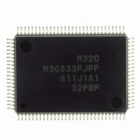
Manufacturer Part Number
M30833FJFP#U3
Description
IC M32C/83 MCU FLASH 100QFP
Manufacturer
Renesas Electronics America
Series
M16C™ M32C/80r
Datasheets
1.M3087BFLGPU3.pdf
(364 pages)
2.M30833FJGPU3.pdf
(96 pages)
3.M30833FJGPU3.pdf
(529 pages)
Specifications of M30833FJFP#U3
Core Processor
M32C/80
Core Size
16/32-Bit
Speed
32MHz
Connectivity
CAN, I²C, IEBus, SIO, UART/USART
Peripherals
DMA, WDT
Number Of I /o
85
Program Memory Size
512KB (512K x 8)
Program Memory Type
FLASH
Ram Size
31K x 8
Voltage - Supply (vcc/vdd)
3 V ~ 5.5 V
Data Converters
A/D 26x10b; D/A 2x8b
Oscillator Type
Internal
Operating Temperature
-40°C ~ 85°C
Package / Case
100-QFP
For Use With
R0K330879S001BE - KIT DEV RSK M32C/87R0K330879S000BE - KIT DEV RSK M32C/87
Lead Free Status / RoHS Status
Lead free / RoHS Compliant
Eeprom Size
-
Available stocks
Company
Part Number
Manufacturer
Quantity
Price


Rev.
REVISION HISTORY
Date
Page
276
277
278
280
281
283
284
285
286
290
291
292
293
294
297
301
308
312
318
322
• Table 21.10 Phase-Delayed Waveform Output Mode Specifications revised
• Figure 21.25 Phase-Delayed Waveform Output Mode modified
• 21.3.3 Set/Reset Waveform Output (SR Waveform Output) Mode revised
• Table 21.11 SR Waveform Output Mode Specifications revised
• Figure 21.26 SR Waveform Output Mode modified
• 21.3.4 Bit-Modulation PWM Output Mode revised
• Table 21.12 Bit Modulation PWM Output Mode revised
• Figure 21.27 Bit Modulation PWM Mode Pulse numbering added
• 21.3.5 Real-Time Port (RTP) Output Mode (Group 2 and 3) revised
• Table 21.14 RTP Output Mode Specifications Note 1 added
• Figure 21.29 Real-Time Port Output Mode modified
• 21.3.6 Parallel Real-Time Port Output Mode (Group 2 and 3) revised
• Table 21.15 Parallel RTP Output Mode Note 1 added
• Figure 21.31 Parallel RTP Output Mode modified
• Figure 21.35 G0EMR to G1EMR Registers and G0ETC to G1ETC Registers
• Figure 21.36 G0ERC to G1ERC Registers Note 1 added
• Figure 21.37 G0IRF to G1IRF Registers and G0TB to G1TB Registers Notes
• Figure 21. 38 G0CMP0 to G0CMP3 Registers, G1CMP0 to G1CMP3
• Table 21.16 Clock Synchronous Serial I/O Mode Specifications (Group 0
• Table 21.22 UART Mode Specifications (Group 0 and 1) Explanation of
• Table 21.28 HDLC Processing Mode Specifications (Group 0 and 1)
• Table 21.30 Variable Clock Synchronous Serial I/O Mode Specifications
• Table 21.36 IE Bus Mode Specification Explanation of transfer clock revised
• Table 21.41 Clock Synchronous Serial I/O Mode (Group 3) Explanation of
CAN
Bit symbols of each register are now capitalized (e.g. Reset0 is changed to
Note 1 added
1 and 2 in G0IRF to G1IRF registers revised; Note 1 added to G0TB to G1TB
registers
Registers, G0MSK0 to G0MSK1 Registers, G1MSK0 to G1MSK1 Registers,
G0TCRC to G1TCRC Registers, and G0RCRC to G1RCRC Registers Note 1
revised and Note 2 added to G0TCRC to G1TCRC registers; Note 3 in G0RCRC
to G1RCRC registers revised
and 1) Explanation of transfer clock revised
transfer clock and Note 2 revised
Explanation of transfer clock revised
(Group 2) Explanation of transfer clock revised
transfer clock revised
RESET0)
M32C/83 GROUP (M32C/83, M32C/83T) Hardware Manual
C-9
Description
Summary
Related parts for M30833FJFP#U3
Image
Part Number
Description
Manufacturer
Datasheet
Request
R

Part Number:
Description:
KIT STARTER FOR M16C/29
Manufacturer:
Renesas Electronics America
Datasheet:

Part Number:
Description:
KIT STARTER FOR R8C/2D
Manufacturer:
Renesas Electronics America
Datasheet:

Part Number:
Description:
R0K33062P STARTER KIT
Manufacturer:
Renesas Electronics America
Datasheet:

Part Number:
Description:
KIT STARTER FOR R8C/23 E8A
Manufacturer:
Renesas Electronics America
Datasheet:

Part Number:
Description:
KIT STARTER FOR R8C/25
Manufacturer:
Renesas Electronics America
Datasheet:

Part Number:
Description:
KIT STARTER H8S2456 SHARPE DSPLY
Manufacturer:
Renesas Electronics America
Datasheet:

Part Number:
Description:
KIT STARTER FOR R8C38C
Manufacturer:
Renesas Electronics America
Datasheet:

Part Number:
Description:
KIT STARTER FOR R8C35C
Manufacturer:
Renesas Electronics America
Datasheet:

Part Number:
Description:
KIT STARTER FOR R8CL3AC+LCD APPS
Manufacturer:
Renesas Electronics America
Datasheet:
Part Number:
Description:
KIT STARTER FOR RX610
Manufacturer:
Renesas Electronics America
Datasheet:

Part Number:
Description:
KIT STARTER FOR R32C/118
Manufacturer:
Renesas Electronics America
Datasheet:

Part Number:
Description:
KIT DEV RSK-R8C/26-29
Manufacturer:
Renesas Electronics America
Datasheet:

Part Number:
Description:
KIT STARTER FOR SH7124
Manufacturer:
Renesas Electronics America
Datasheet:

Part Number:
Description:
KIT STARTER FOR H8SX/1622
Manufacturer:
Renesas Electronics America
Datasheet:

Part Number:
Description:
KIT DEV FOR SH7203
Manufacturer:
Renesas Electronics America
Datasheet: